
Model compensating method for controlling thin film deposition rate in physical gaseous phase thin film deposition process
A thin-film deposition and physical gas phase technology, applied in the field of microelectronics, can solve the problems of material intrinsic performance device characteristics deviating from design requirements, affecting the precise control of thin-film thickness, and reducing the efficiency of machine use, etc. The effect of stable microstructure and performance and guaranteed accuracy
Patent Information
- Authority / Receiving Office
- CN · China
- Patent Type
- Patents(China)
- Current Assignee / Owner
- Publication Date
- 2013-07-31
Smart Images
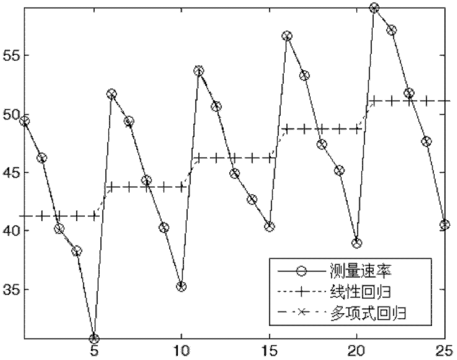
Figure 1 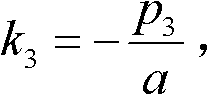
Figure 2 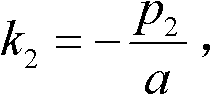
Figure 3
Abstract
Description
technical field
[0001] The invention belongs to the technical field of microelectronics, and in particular relates to a method for controlling the film deposition rate of a physical vapor deposition process. Background technique
[0002] The physical vapor phase thin film deposition process is usually used to prepare high-quality conductive thin film materials, which require precise control of film thickness and material properties. However, the deposition rate of the film will deviate significantly with the consumption of the target material, which will affect the precise control of the film thickness, and cause the intrinsic performance of the material and its device characteristics to deviate from the design requirements. In the existing technology, real-time monitoring and dynamic compensation of the deposition rate of the film is an effective method to obtain a stable film deposition rate, but the cost of this dynamic feedback compensation system is high, and the online...
Examples
Embodiment 1
[0064] In the vacuum thermal evaporation coating process heated by resistance, the heating current I is used as the compensation object process parameter X, that is, X=I, the source material consumption and I 2 are linearly related, so T is defined as
[0065] T = ∫ 0 t Ydt = ∫ 0 t I 2 dt
[0066] The mathematical model of film deposition rate R that needs to be established has the following form:
[0067] R=aI+p 3 T 3 +p 2 T 2 +p 1 T+R 0
[0068] According to the test machine data, perform linear regression and polynomial regression through the Matlab program, and obtain the corresponding regression coefficients: a, p 3 ,p 2 ,p 1 and R 0 .
[0069] Compensation coefficient k 3 、k 2 、k 1 :
[0070] k 3 = - ...
Embodiment 2
[0077] In the DC magnetron sputtering coating process, through the joint action of voltage and magnetic field, ionized inert gas Ar ions are used to bombard the target to generate ions, atoms or molecules, which are deposited on the substrate to form a thin film. In addition to using DC power P as the compensation target process parameter, if the magnetic field strength B can be automatically controlled and recorded, it is also possible to use the process parameters related to the magnetic field as the compensation target process parameter. This compensation method is expected to increase the utilization rate of source materials . Since target consumption is dependent on both electric power and magnetic field strength, the integral object Y can take the product of the two.
[0078] The compensation object process parameter X and the historical record parameter T are respectively defined as:
[0079] X = B;
[0080] T = ∫ 0...