
Single crystal battery and preparation method thereof
A single crystal and battery technology, applied in the manufacture of circuits, electrical components, final products, etc., can solve problems such as low power efficiency, poor potential-induced attenuation effect, and poor light-induced attenuation effect
Patent Information
- Authority / Receiving Office
- CN · China
- Current Assignee / Owner
- Publication Date
- 2021-07-16
Smart Images
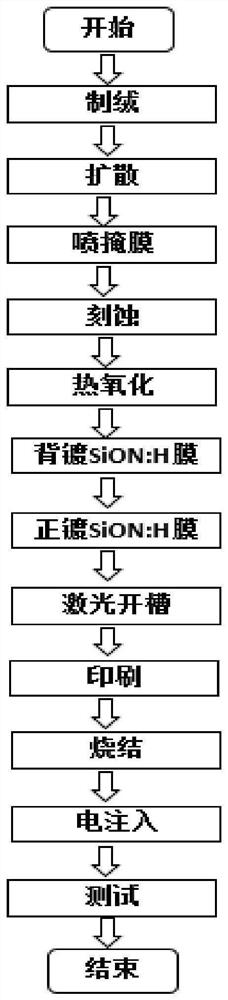
Figure 1 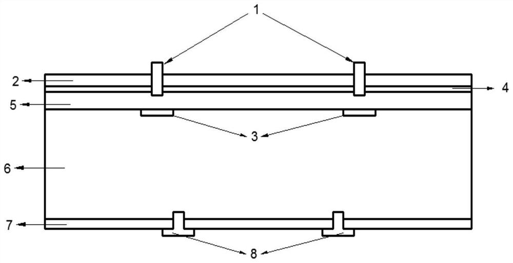
Figure 2 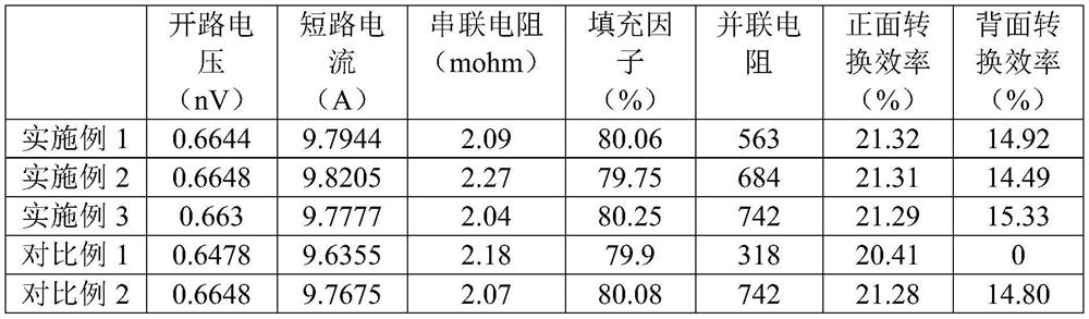
Figure 3
Abstract
Description
technical field
[0001] The invention belongs to the technical field of photovoltaics, and relates to a single crystal battery and a preparation method thereof. Background technique
[0002] Conventional fossil fuels are being exhausted day by day. Among the existing sustainable energy sources, solar energy is undoubtedly the cleanest, most common and most potential alternative energy source. Solar power generation devices, also known as solar cells or photovoltaic cells, can directly convert solar energy into electrical energy. The principle of power generation is based on the photovoltaic effect of semiconductor PN junctions.
[0003] The preparation method of the existing commercial conventional monocrystalline cell includes the following steps: 1. Use a trough-type alkaline solution to make a "pyramid" suede; 2. Use a low-pressure tubular diffusion furnace to make a PN junction on the front side of the silicon wafer; 3. Use a chain-type Acid etching to remove the surroun...
Examples
Embodiment 1
[0077] In this example, a monocrystalline battery is prepared according to the following method:
[0078] a) 10,000 pieces of silicon wafers of the single crystal M2 type are used, and the silicon wafers are etched with alkaline solution to make suede;
[0079] b) Put the textured silicon wafer into the low-pressure diffusion furnace equipment, pass the phosphorus source to make a PN junction, and control the square resistance to 70Ω;
[0080] c) Spray a paraffin mask on a part of the surface of the silicon wafer using mask spraying equipment, and the pattern of this mask is consistent with the pattern of the metal grid lines printed on the front side of the subsequent silicon wafer;
[0081] d) In the chain-type acid polishing and etching equipment, spray the masked silicon wafer in some areas of step c), first use hydrofluoric acid to remove the PN junction around the silicon wafer and the back side, and then soak the silicon wafer in hydrofluoric acid and Remove the oxide ...
Embodiment 2
[0093] In this example, a monocrystalline battery is prepared according to the following method:
[0094] a) 10,000 pieces of silicon wafers of the single crystal M2 type are used, and the silicon wafers are etched with alkaline solution to make suede;
[0095] b) Put the textured silicon wafer into the low-pressure diffusion furnace equipment, pass the phosphorus source to make a PN junction, and control the square resistance at 75Ω;
[0096] c) Spray a paraffin mask on a part of the surface of the silicon wafer using mask spraying equipment, and the pattern of this mask is consistent with the pattern of the metal grid lines printed on the front side of the subsequent silicon wafer;
[0097] d) In the chain-type acid polishing and etching equipment, spray the masked silicon wafer in some areas of step c), first use hydrofluoric acid to remove the PN junction around the silicon wafer and the back side, and then soak the silicon wafer in hydrofluoric acid and Remove the oxide ...
Embodiment 3
[0108] In this example, a monocrystalline battery is prepared according to the following method:
[0109] a) 10,000 pieces of silicon wafers of the single crystal M2 type are used, and the silicon wafers are etched with alkaline solution to make suede;
[0110] b) Put the textured silicon wafer into the low-pressure diffusion furnace equipment, pass the phosphorus source to make a PN junction, and control the square resistance at 80Ω;
[0111] c) Spray a paraffin mask on a part of the surface of the silicon wafer using mask spraying equipment, and the pattern of this mask is consistent with the pattern of the metal grid lines printed on the front side of the subsequent silicon wafer;
[0112] d) In the chain-type acid polishing and etching equipment, spray the masked silicon wafer in some areas of step c), first use hydrofluoric acid to remove the PN junction around the silicon wafer and the back side, and then soak the silicon wafer in hydrofluoric acid and Remove the oxide ...