Ultrasonic imaging device

一种成像装置、超声波的技术,应用在测量装置、声波的再辐射、使用声波/超声波/次声波分析固体等方向,能够解决连接端子面积小、难被检测物体内部检测、异常判定能力不足等问题

Inactive Publication Date: 2009-02-11
KK TOSHIBA
View PDF7 Cites 6 Cited by
  • Summary
  • Abstract
  • Description
  • Claims
  • Application Information

AI Technical Summary

Problems solved by technology

[0004] This detection method has the following problems at the same time: the mechanical scanning immersed in water is laborious and time-consuming, and when detecting semiconductor chips, etc., the chips cannot be used after detection, and the connection terminal area of ​​the semiconductor chip to be detected is getting smaller and smaller, and the pitch It is getting narrower and narrower, and the abnormal judgment ability may be insufficient under the current detection accuracy
[0012] However, since the piezoelectric conversion element is immersed in liquid in the water immersion method, the liquid easily penetrates into the piezoelectric conversion element, reducing its durability.
And it is difficult to internally detect the object to be detected arranged in a closed container from the outside

Method used


Image

  • Ultrasonic imaging device
  • Ultrasonic imaging device
  • Ultrasonic imaging device

Examples


no. 1 Embodiment

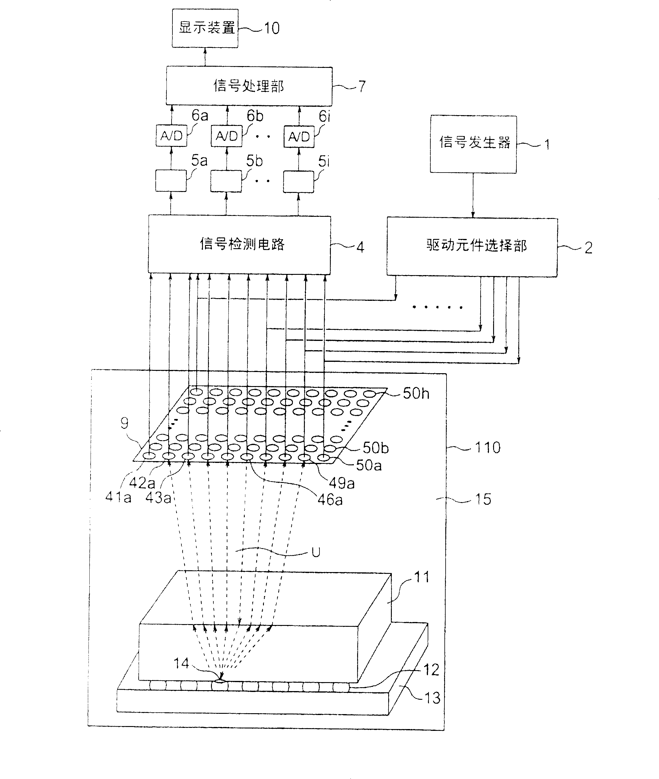
[0087] figure 1 It is a structural diagram explaining the structure of the ultrasonic detection apparatus concerning the 1st Example of this invention. Such as figure 1 As shown, the ultrasonic detection device includes: ultrasonic transducer 9; signal generating part 1; drive element selection part 2; signal detection circuit 4; amplifiers 5a, 5b, ..., 5i; , 6i; the signal processing unit 7, the display device 10, and the detection container 110. Water 15 is accommodated in the detection container 110, and the ultrasonic transducer 9, the semiconductor chip 11, the wiring substrate 13, and the connecting solder 12 (hereinafter referred to as the semiconductor chip) as the detection object (ultrasonic detection object) are arranged immersed in the water 15. 11. The wiring substrate 13 and the connecting solder 12 are collectively referred to as the semiconductor chip 11, etc.).

[0088] The ultrasonic transducer 9 is a device in which a plurality of piezoelectric conversion...

no. 2 Embodiment

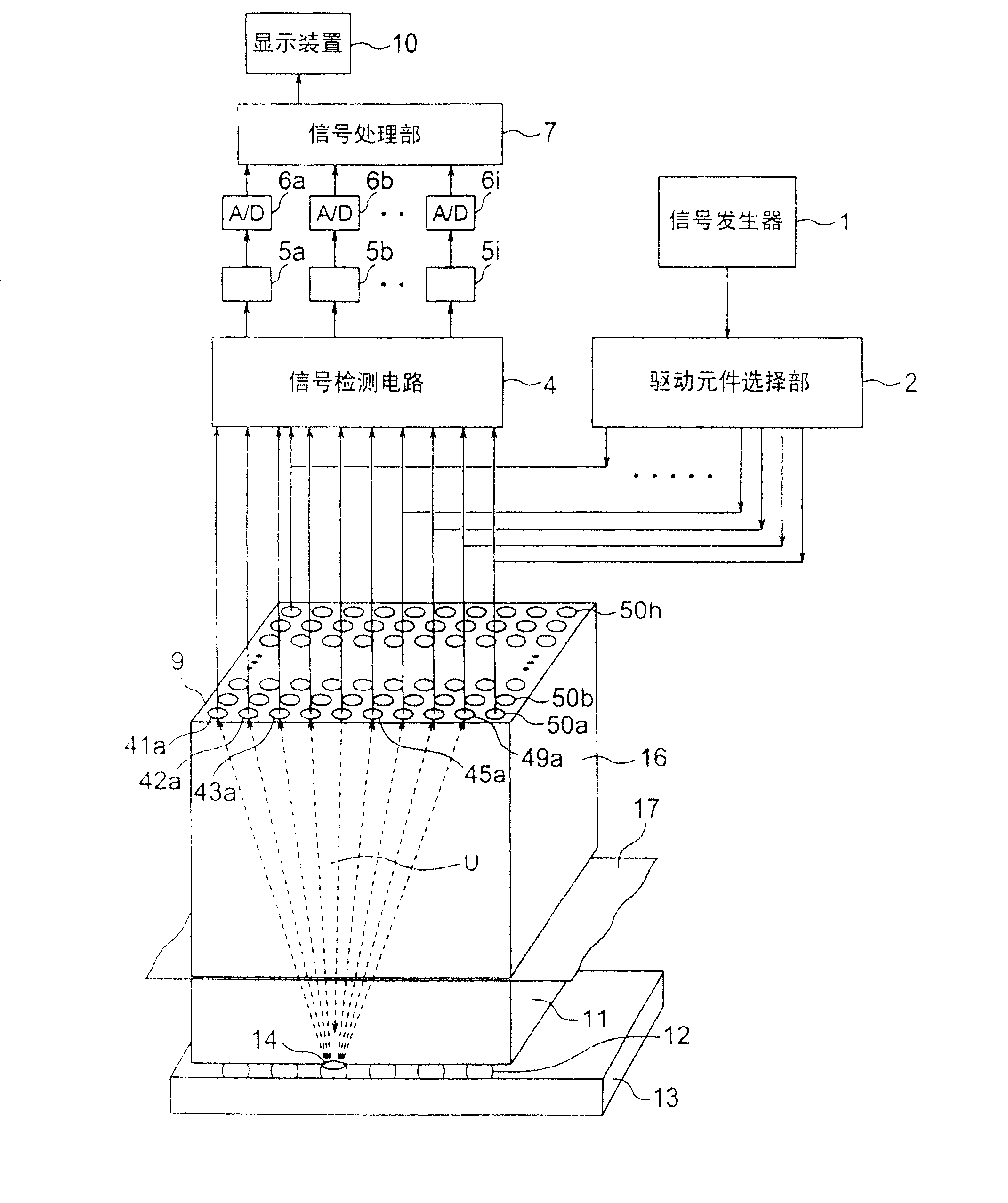
[0102] image 3 It is a figure explaining the structure of the ultrasonic detection apparatus concerning the 2nd Example of this invention. exist image 3 In , components that have already been described are given the same numbers, and descriptions of the components and operations are omitted. This embodiment differs from the above-mentioned first embodiment in that the object to be detected is irradiated with ultrasonic waves not by water but by using a block material.

[0103] Such as image 3 As shown, the ultrasonic transducer 9 is constructed with a shoe material 16 as a substrate. Further, the block 16 is provided with a coupling medium 17 on its back surface, and the semiconductor chip 11 or the like to be detected is pressed by the coupling medium 17 . The bulk material 16 is made of the same material as that of the semiconductor chip 11 (for example, silicon, epoxy resin, ceramics, etc.). The coupling medium 17 may be of the material and thickness already describ...

no. 3 Embodiment

[0108] Figure 4 It is a configuration diagram illustrating the configuration of an ultrasonic testing device related to an embodiment of the present invention. exist Figure 4 In , the components already described are given the same numbers, and their structures and operations are omitted. In this embodiment, the piezoelectric conversion element is directly formed on the back surface (opposite to the functional surface) of the semiconductor chip 11a to be tested, and its upper electrode is contacted through the contact terminal to supply the driving voltage and take out the generated voltage.

[0109] Such as Figure 4 As shown, a common electrode 58 is formed on the back surface of the semiconductor chip 11a by, for example, sputtering, and piezoelectric layers 60a, 60b, 60c, 60d, . . . are formed in a matrix on the common electrode 58 . Upper electrodes 59a, 59b, 59c, 59d, . . . are formed on the piezoelectric layer 60a and the like. For example, the piezoelectric layer...


PUM


Abstract

An ultrasonograph, an ultrasonic transducer, an inspection device, and an ultrasonic imaging device enabling easy and quick inspection and high-resolution or high-speed processing are provided. Barium titanate (BaTiO3) or lead zirconate titanate (PZT) is used for a piezoelectric material constituting the ultrasonic transducer, and the thickness thereof is 0.1 mum to 100 mum. Included therein are a drive section capable of driving an arbitrary one of piezoelectric layers, a detecting section detecting electrical signals generated by the plural piezoelectric layers based on echoes from an irradiation object, the echoes being originated from an ultrasonic wave generated by the driven piezoelectric layer, and a processing section performing processing for visualizing a state of the irradiation object based on the detected electrical signals.

Description

technical field [0001] The present invention relates to an ultrasonic imaging device that uses ultrasonic waves to detect internal defects and abnormalities such as peeling of semiconductor chips, metals, ceramic parts, resins, etc. Background technique [0002] Ultrasonic inspection of microscopic internal structures such as semiconductor chips (integrated circuits: ICs) is intended to detect the bonding state of solder bonding the functional surfaces of semiconductor chips and wiring boards and fillers filling gaps between them. [0003] One such detection method is as follows: while the monocular ultrasonic transducer is mechanically scanned in water, ultrasonic waves are irradiated from the transducer through the water to the detection object, and the ultrasonic wave that propagates through the detection object and becomes an echo return is detected using the above-mentioned transducer. Capture, process the resulting signal, and judge the state of the detection object. ...

Claims


Application Information

Patent Timeline
Patent Type & Authority Patents(China)
IPC IPC(8): G01N29/24B06B1/06G01N29/06G01N29/28G01S15/89H01L41/083
CPCG01N2291/0423G01N29/2418G01N29/28B06B1/0622G01N29/06G01N29/2437G01N2291/106G01N29/24
Inventor 唐泽博一中本正幸落合诚福田胜义平泽泰治池田贤弘
Owner KK TOSHIBA
Why Eureka
Try Eureka