Ultrasonic examining instrument

A detection device, ultrasonic technology, applied to measuring devices, using sound waves/ultrasonic waves/infrasonic waves to analyze solids, frequency/direction characteristic devices, etc., can solve the problems of unusable chips, reduced durability, laborious and time-consuming mechanical scanning, etc.

Inactive Publication Date: 2009-05-20
KK TOSHIBA
View PDF7 Cites 0 Cited by
  • Summary
  • Abstract
  • Description
  • Claims
  • Application Information

AI Technical Summary

Problems solved by technology

[0005] This detection method has the following problems at the same time: the mechanical scanning immersed in water is laborious and time-consuming, and when detecting semiconductor chips, etc., the chips cannot be used after detection, and the connection terminal area of ​​the semiconductor chip to be detected is getting smaller and smaller, and the pitch It is getting narrower and narrower, and the abnormal judgment ability may be insufficient under the current detection accuracy
[0013] However, since the piezoelectric conversion element is immersed in liquid in the water immersion method, the liquid easily penetrates into the piezoelectric conversion element, reducing its durability.
And it is difficult to internally detect the object to be detected arranged in a closed container from the outside

Method used


Image

  • Ultrasonic examining instrument
  • Ultrasonic examining instrument
  • Ultrasonic examining instrument

Examples


no. 1 Embodiment

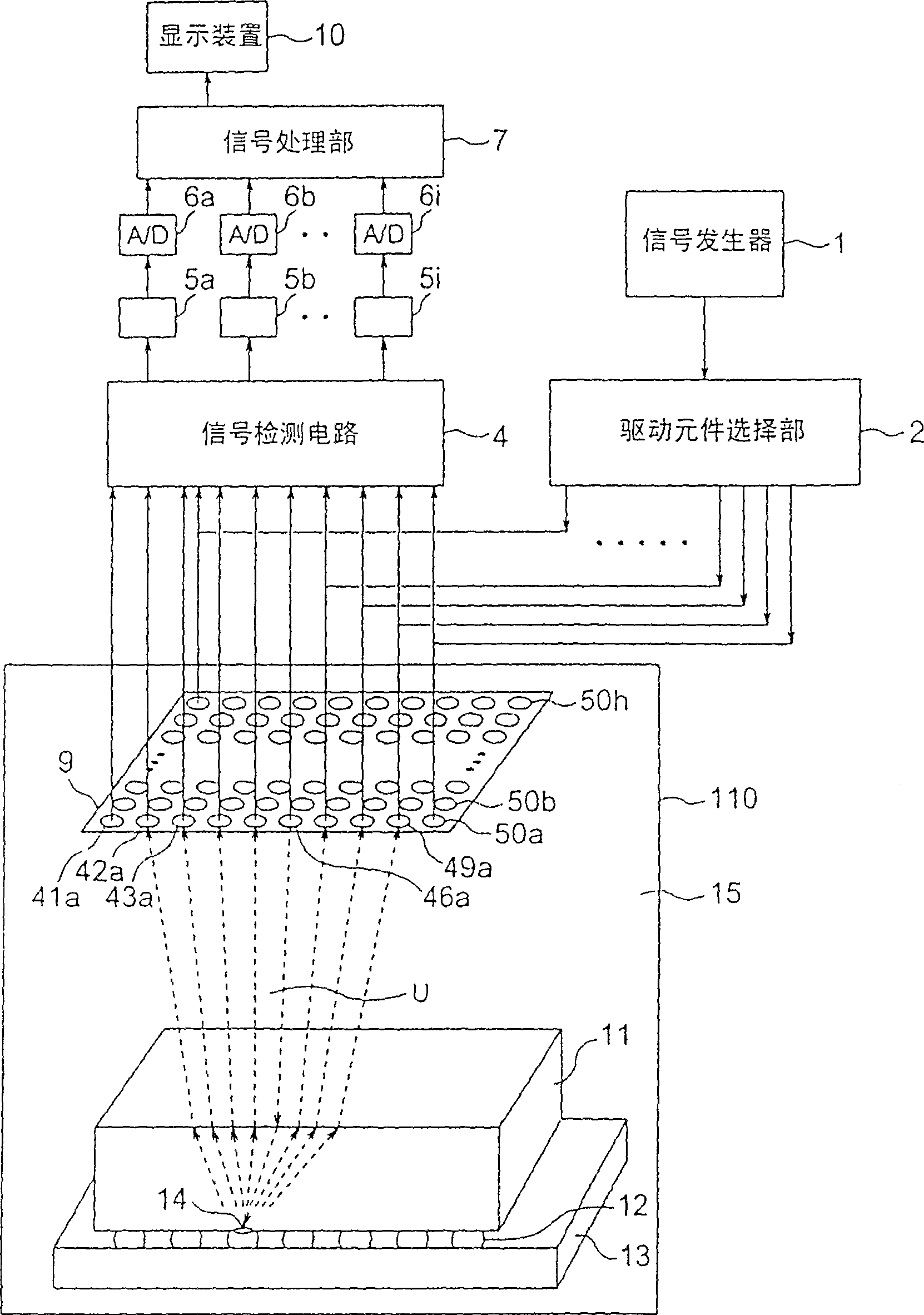
[0068] figure 1 It is a structural diagram explaining the structure of the ultrasonic detection apparatus concerning the 1st Example of this invention. like figure 1 As shown, the ultrasonic detection device includes: ultrasonic transducer 9; signal generating part 1; drive element selection part 2; signal detection circuit 4; amplifiers 5a, 5b, ..., 5i; , 6i; the signal processing unit 7, the display device 10, and the detection container 110. Water 15 is accommodated in the detection container 110, and the ultrasonic transducer 9, the semiconductor chip 11, the wiring substrate 13, and the connecting solder 12 (hereinafter referred to as the semiconductor chip) as the detection object (ultrasonic detection object) are arranged immersed in the water 15. 11. The wiring substrate 13 and the connecting solder 12 are collectively referred to as the semiconductor chip 11, etc.).

[0069] The ultrasonic transducer 9 is a device in which a plurality of piezoelectric conversion el...

no. 2 Embodiment

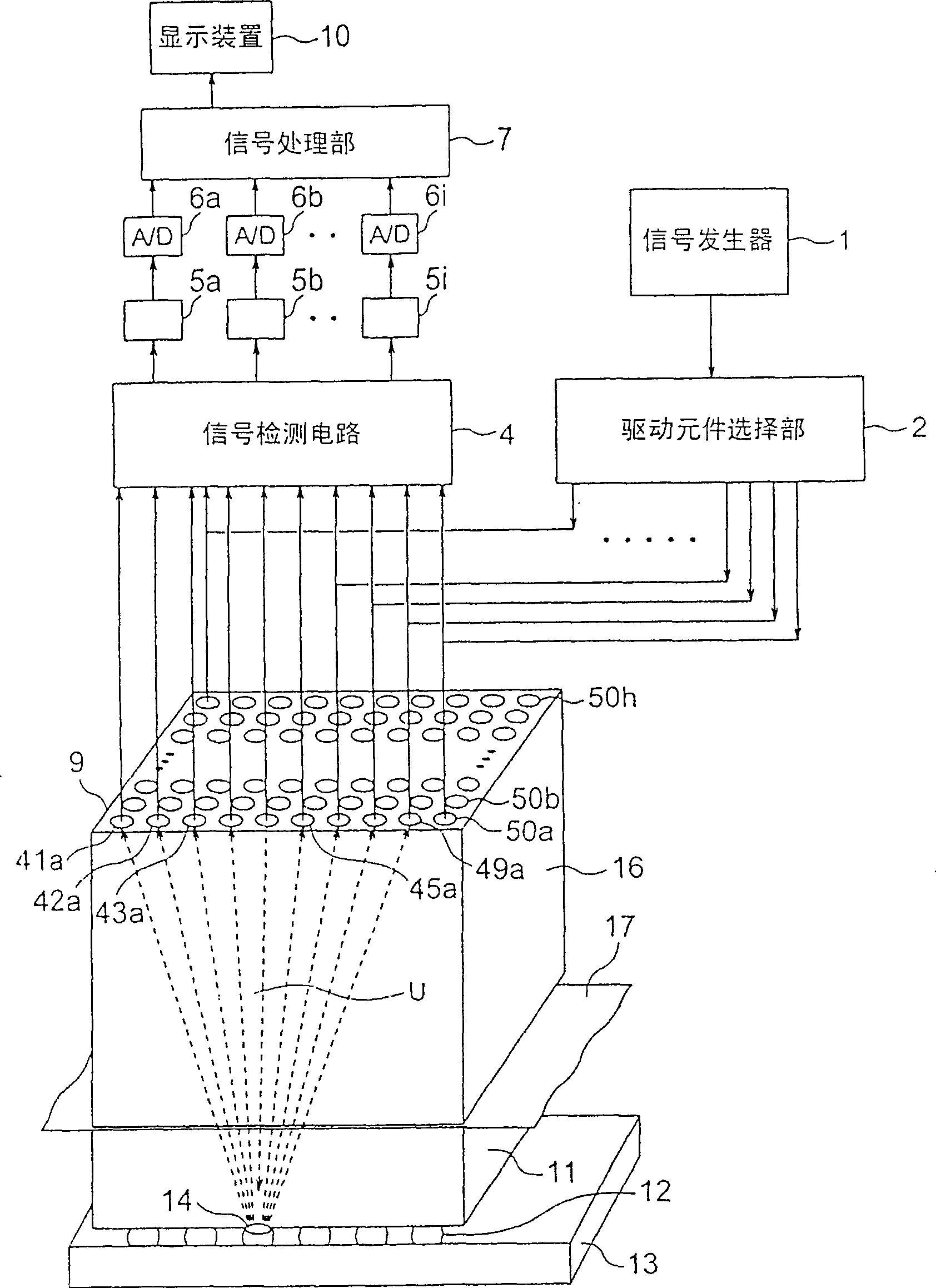
[0083] image 3 It is a figure explaining the structure of the ultrasonic detection apparatus concerning the 2nd Example of this invention. exist image 3 In , components that have already been described are given the same numbers, and descriptions of the components and operations are omitted. This embodiment differs from the above-mentioned first embodiment in that the object to be detected is irradiated with ultrasonic waves not by water but by using a block material.

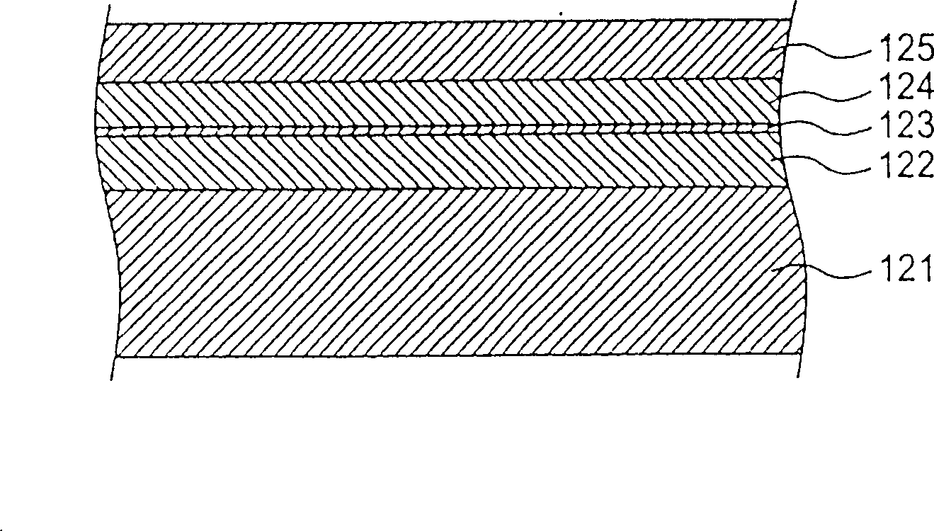
[0084] like image 3 As shown, the ultrasonic transducer 9 is constructed with a shoe material 16 as a substrate. Further, the block 16 is provided with a coupling medium 17 on its back surface, and the semiconductor chip 11 or the like to be detected is pressed by the coupling medium 17 . The bulk material 16 is made of the same material as that of the semiconductor chip 11 (for example, silicon, epoxy resin, ceramics, etc.). The coupling medium 17 may be of the material and thickness already described,...

no. 3 Embodiment

[0089] Figure 4 It is a configuration diagram illustrating the configuration of an ultrasonic testing device related to an embodiment of the present invention. exist Figure 4 In , the components already described are given the same numbers, and their structures and operations are omitted. In this embodiment, the piezoelectric conversion element is directly formed on the back surface (opposite to the functional surface) of the semiconductor chip 11a to be tested, and its upper electrode is contacted through the contact terminal to supply the driving voltage and take out the generated voltage.

[0090] like Figure 4 As shown, a common electrode 58 is formed on the back surface of the semiconductor chip 11a by, for example, sputtering, and piezoelectric layers 60a, 60b, 60c, 60d, . . . are formed in a matrix on the common electrode 58 . Upper electrodes 59a, 59b, 59c, 59d, . . . are formed on the piezoelectric layer 60a and the like. For example, the piezoelectric layer 60...


PUM


Abstract

The present invention provides an ultrasonic inspecting apparatus capable of easily and speedily performing inspection with high resolution. The ultrasonograph comprises: a laser beam source generating an intermittent or intensity-modulated laser beam; an irradiation optical system irradiating an irradiation object with the generated laser beam in a spot-like state; a scan-moving mechanism scan-moving the irradiation optical system relatively to the irradiation object; a vibration displacement detecting section which performs non-contact detection of vibration displacement on a surface of the irradiation object by a displacement measuring method using a laser beam, the vibration displacement caused by an echo of an ultrasonic wave in the irradiation object generated by the irradiated laser beam, and which transduces the vibration displacement to an electrical signal; and a processing section performing processing for visualizing a state of the irradiation object based on the electrical signal obtained after the transducing and a position of the scan-moved irradiation optical system.

Description

[0001] The present invention is a divisional application of Chinese Patent Application No. 02802634.9, which entered the national phase on April 10, 2003, entitled "ultrasonic detection device, ultrasonic transducer, detection device, and ultrasonic imaging device". technical field [0002] The present invention relates to an ultrasonic testing device that uses ultrasonic waves to detect internal defects and abnormalities such as peeling of semiconductor chips, metals, ceramic parts, resins, etc. Background technique [0003] Ultrasonic inspection of microscopic internal structures such as semiconductor chips (integrated circuits: ICs) is intended to detect the bonding state of solder bonding the functional surfaces of semiconductor chips and wiring boards and fillers filling gaps between them. [0004] One such detection method is as follows: while the monocular ultrasonic transducer is mechanically scanned in water, ultrasonic waves are irradiated from the transducer throug...

Claims


Application Information

Patent Timeline
Patent Type & Authority Patents(China)
IPC IPC(8): G01N29/06G01N29/04B06B1/06G01N29/00G01N29/24H04R1/34
Inventor 唐泽博一中本正幸落合诚福田胜义平泽泰治池田贤弘
Owner KK TOSHIBA
Why Eureka
Try Eureka