
Electroluminescent display device

A technology for display devices and light-emitting elements, which is applied to electroluminescent light sources, electric light sources, lighting devices, etc., can solve the problem of not allowing the current ratio to increase or decrease, and achieve the effect of good display uniformity

Inactive Publication Date: 2007-11-21
KONINKLIJKE PHILIPS ELECTRONICS NV
View PDF1 Cites 0 Cited by
  • Summary
  • Abstract
  • Description
  • Claims
  • Application Information

AI Technical Summary

Problems solved by technology

However, this method does not allow the current to be scaled between the two time periods

Method used


Image

  • Electroluminescent display device
  • Electroluminescent display device
  • Electroluminescent display device

Examples


Embodiment Construction

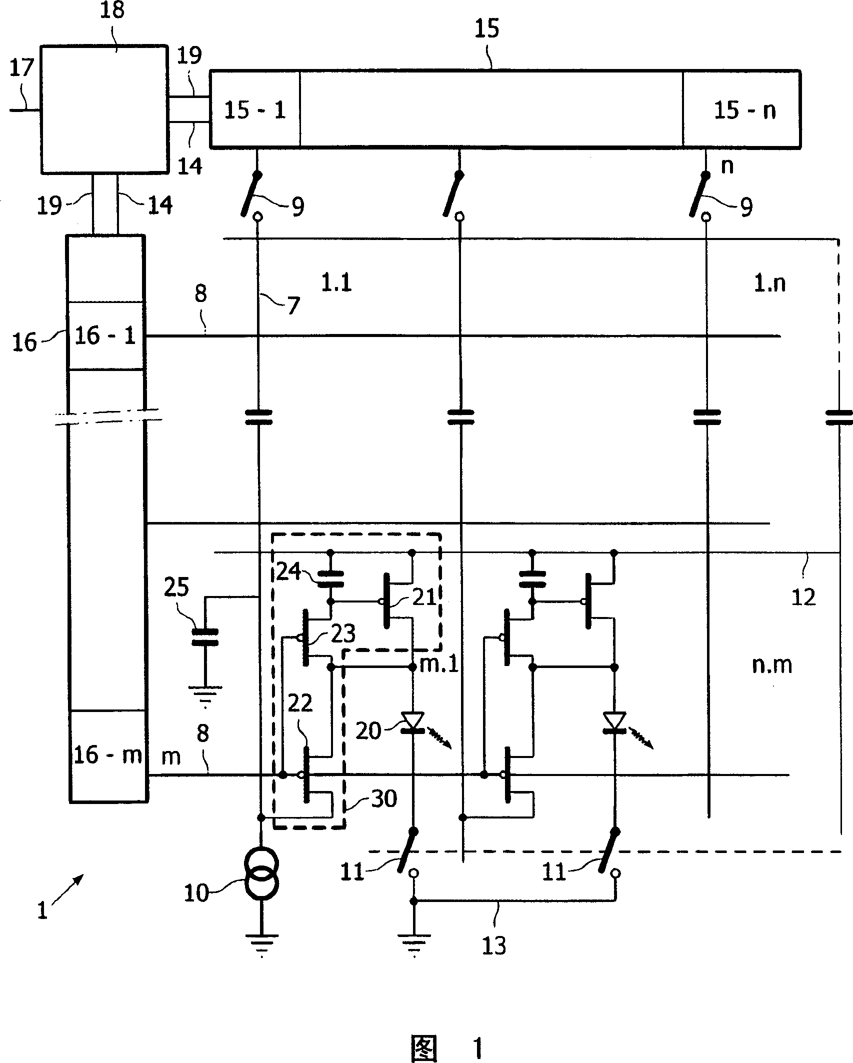
[0024] FIG. 1 schematically shows an equivalent circuit diagram of a part of a display device 1 according to the invention. The display device comprises a matrix of (P)LEDs or (O)LEDs 20 having n rows or rows 8 (1, 2, . . . , m) and m columns 7 (1, 2, . . . , n). Where rows and columns are mentioned, the rows and columns may be interchanged if desired. The device also includes a row selection circuit 16 and a data register 15 . The externally presented information 17, such as a video signal, is processed in a processing unit 18 which charges the individual parts 15-1,...,15-n of the data register 15 via the power line 19 according to the information to be displayed .

[0025] Via line 8 (in this example the gate electrode of a TFT transistor or MOS transistor 22 , by supplying it with the required selection voltage), selection of a row is effected by means of a row selection circuit 16 .

[0026] In this prior art device the data is written by current programming, which mea...


PUM


Abstract

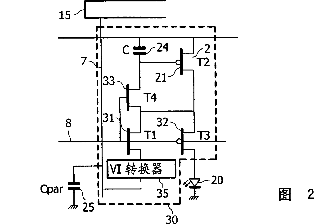
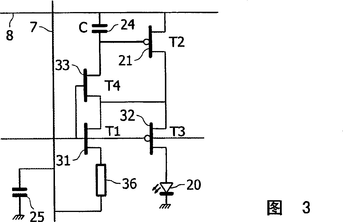
The use of a resistive or capacitive voltage-current -converter (35) in an (active addressed matrix) luminescent display pixel circuit allows fast programming and highly accurate pixel current definition for improved display uniformity.

Description

technical field [0001] The present invention relates to a display device including pixels in the intersecting electrode area, each pixel at least includes a current adjustment circuit based on a storage element, and the connection point of the adjustment circuit can be connected in series with a light emitting element. [0002] Such electroluminescent-based display devices are increasingly based on (polymeric) semiconducting organic materials, semiconducting inorganic materials or electroluminescent materials. Such a display device can emit light by segmented pixels (or a fixed pattern), and it is also possible to display with a matrix pattern. The adjustment of the pixel by the storage element determines the intensity of the pixel's light emission. The adjustment by means of storage elements is increasingly being used in areas where additional switching elements are used in the adjustment (so-called active drive). [0003] Suitable fields of application of such display devi...

Claims


Application Information

Patent Timeline
IPC IPC(8): G09G3/32
CPCG09G2300/0852G09G2310/0259G09G2300/0861G09G2300/0842G09G3/325G09G2300/0809G09G2320/0252G09G3/30G09G3/20H05B33/12G09G3/32
Inventor A·森佩尔
Owner KONINKLIJKE PHILIPS ELECTRONICS NV
Learn More