
Semiconductor device with high-frequency interconnection

A semiconductor, high-frequency technology, applied in the direction of semiconductor devices, semiconductor/solid-state device components, electric solid-state devices, etc., can solve problems such as changes in the transmission characteristics of high-frequency interconnection 101, and achieve the effect of suppressing eddy currents

Inactive Publication Date: 2013-05-01
RENESAS ELECTRONICS CORP
View PDF1 Cites 0 Cited by
  • Summary
  • Abstract
  • Description
  • Claims
  • Application Information

AI Technical Summary

Problems solved by technology

Therefore, the circuit constant of the high-frequency interconnection 101 fluctuates, resulting in a change in the transmission characteristics of the high-frequency interconnection 101

Method used


Image

  • Semiconductor device with high-frequency interconnection
  • Semiconductor device with high-frequency interconnection
  • Semiconductor device with high-frequency interconnection

Examples


no. 1 example

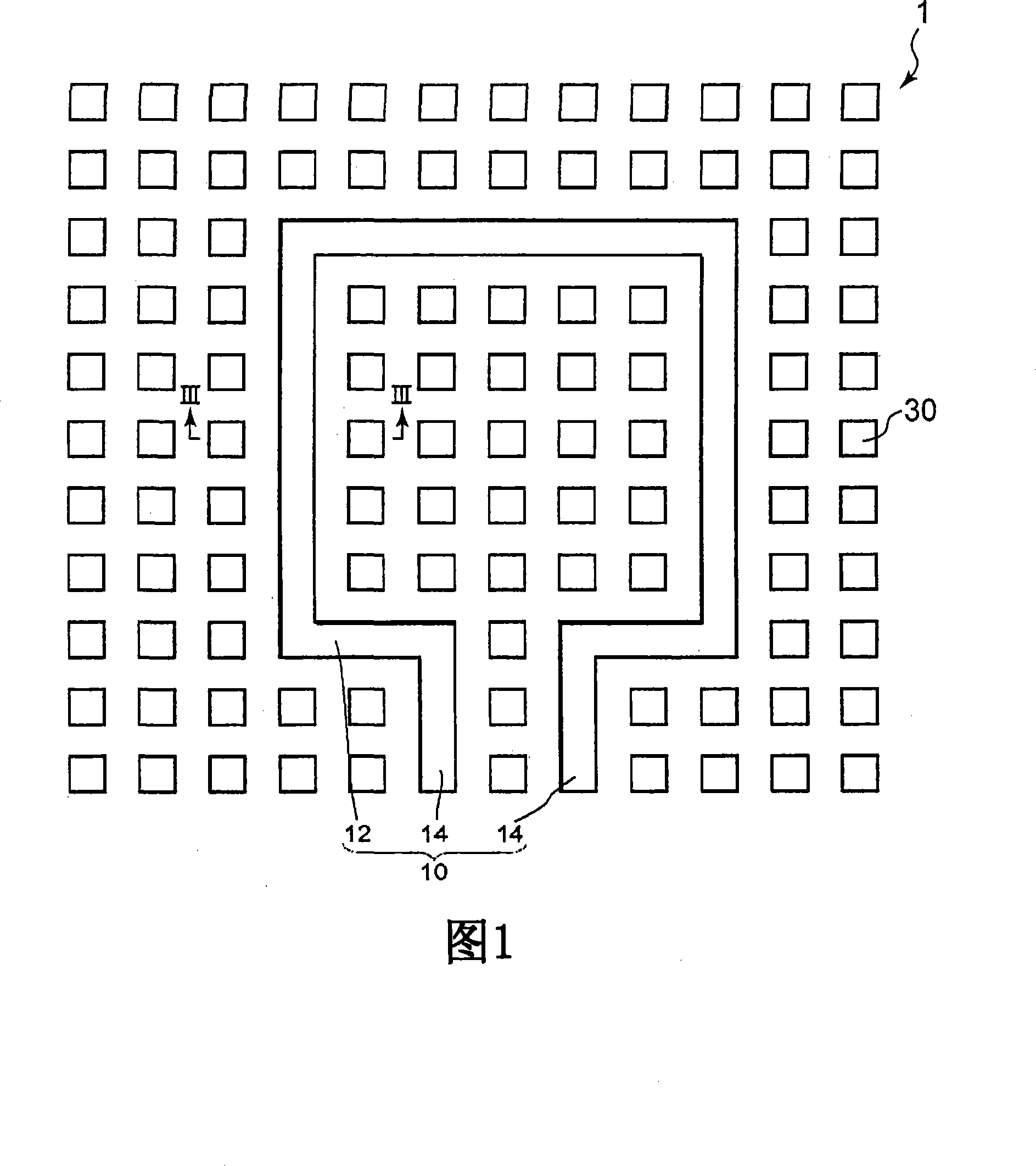
[0029] figure 1 with 2 Each shows a plan view of the semiconductor device according to the first embodiment of the present invention. The semiconductor device 1 includes a high-frequency interconnection 10 and a dummy conductor pattern 20 (second dummy conductor pattern). For example, a current having a frequency of 5 GHz or higher flows through the high-frequency interconnect 10. The high-frequency interconnection 10 includes an interconnection, which is formed in the shape of a coil and functions as an inductor 12. The high frequency interconnect 10 further includes an extraction interconnect 14 which is connected to the coil-shaped inductor 12.

[0030] A plurality of dummy conductor patterns 20 are provided near the high-frequency interconnection 10. Note that the dummy conductor pattern 20 is provided in a different layer from the high-frequency interconnection 10. figure 1 with 2 The layer provided with the high-frequency interconnection 10 (first layer) and the layer p...

no. 2 example

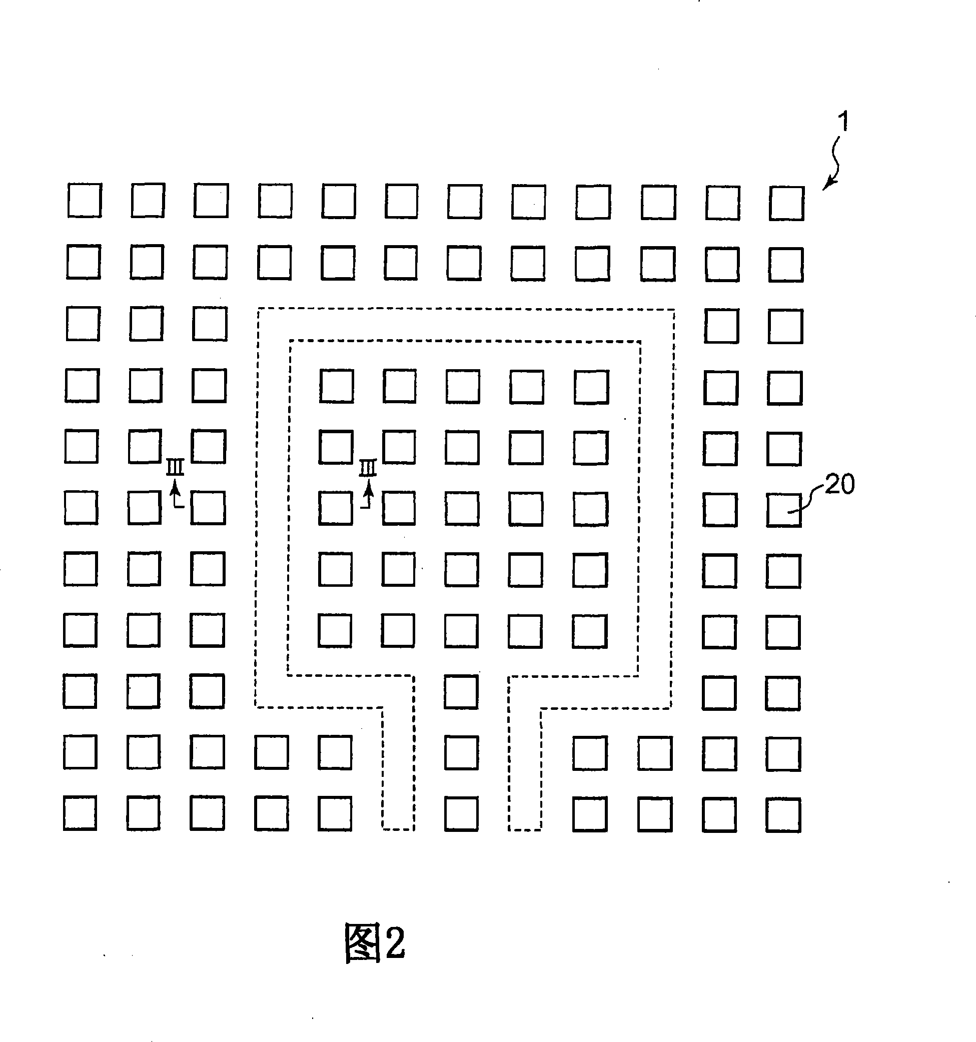
[0044] Picture 10 with 11 Each shows a plan view of a semiconductor device according to the second embodiment of the present invention. In this embodiment, Picture 11 The layer shown in (the second layer) is set next to Picture 10 Below the layer (first layer) shown in. The semiconductor device of the second embodiment includes a high-frequency interconnect 10 and a dummy conductor pattern 20 (second dummy conductor pattern). For example, a current having a frequency of 5 GHz or higher flows through the high-frequency interconnect 10. The high-frequency interconnection 10 includes an interconnection, which is formed in a coil shape and functions as an inductor 12. The high frequency interconnect 10 further includes an extraction interconnect 14. One end of the extraction interconnection 14 is connected to the coil-shaped inductor 12. The other end of the extraction interconnect 14 is connected to, for example, an electrode pad, or a source / drain region of a transistor.

[...


PUM


Abstract

Provided is a semiconductor device including high-frequency interconnect and dummy conductor patterns (second dummy conductor patterns). The dummy conductor patterns are disposed in a interconnect layer different from a interconnect layer in which the high-frequency interconnect is disposed. The dummy conductor patterns are disposed so as to keep away from a region overlapping the high-frequency interconnect in plan view. The semiconductor device further includes dummy conductor patterns (first dummy conductor patterns) in the interconnect layer in which the high-frequency interconnect is disposed.

Description

Technical field [0001] The present invention relates to a semiconductor device, and more specifically, to a semiconductor device having high-frequency interconnections and dummy conductor patterns. Background technique [0002] Figure 7 with 8 Each shows a plan view of a semiconductor device according to the prior art. In the semiconductor device 100, the dummy conductor patterns 102 and 103 are provided in the vicinity of the high-frequency interconnection 101. Figure 7 Shows the layer forming the high frequency interconnect 101, and Picture 8 Another layer is shown. in Picture 8 , The area overlapping with the high-frequency interconnect 101 is indicated by a broken line in a plan view. [0003] The dummy conductor pattern 102 is provided in the same layer as the high-frequency interconnection 101, and the dummy conductor pattern 103 is provided in a layer different from the layer where the high-frequency interconnection 101 is provided. The dummy conductor pattern is provide...

Claims


Application Information

Patent Timeline
Patent Type & Authority Patents(China)
IPC IPC(8): H01L23/528
CPCH01L2924/0002H01L23/585H01L23/5227H01L23/535H01L23/66H01L23/522H01L2924/00
Inventor 中柴康隆
Owner RENESAS ELECTRONICS CORP
Features
  • Generate Ideas
  • Intellectual Property
  • Life Sciences
  • Materials
  • Tech Scout
  • Unparalleled Data Quality
  • Higher Quality Content
  • 60% Fewer Hallucinations
Learn More