Check patentability & draft patents in minutes with Patsnap Eureka AI!

Method for reducing polycrystalline silicon loss in mask etching process

A polysilicon and polysilicon layer technology, which is applied in semiconductor/solid-state device manufacturing, electrical components, semiconductor devices, etc., can solve problems such as poor charge bearing capacity and unstable electrical performance of flash memory devices, achieve good electrical performance, and reduce polysilicon loss. Effect

Active Publication Date: 2012-05-23
SHANGHAI HUAHONG GRACE SEMICON MFG CORP
View PDF6 Cites 0 Cited by
  • Summary
  • Abstract
  • Description
  • Claims
  • Application Information

AI Technical Summary

Problems solved by technology

With the development of technology and the reduction of the size of flash memory devices, the thickness of the floating gate polysilicon also becomes thinner. For example, the thickness of the initial polysilicon layer 22 becomes about 300 angstroms. Due to the effect of etching, the final thickness of the floating gate polysilicon The thickness may be less than 100 angstroms. The floating gate polysilicon with such a thickness has a poor ability to withstand charges. At the same time, due to the error of tens of angstroms in the process, its thickness relative to the entire floating gate varies greatly, thus causing the electrical performance of the flash memory device. unstable

Method used


Image

  • Method for reducing polycrystalline silicon loss in mask etching process
  • Method for reducing polycrystalline silicon loss in mask etching process
  • Method for reducing polycrystalline silicon loss in mask etching process

Examples


Embodiment Construction

[0025] In order to better understand the technical content of the present invention, specific embodiments are given together with the attached drawings for description as follows.

[0026] Please refer to image 3 , image 3 Shown is a flowchart of a method for reducing polysilicon loss during mask etching process according to a preferred embodiment of the present invention. The present invention proposes a method for reducing polysilicon loss in a mask etching process, which is applied to the fabrication of floating gates of flash memory devices. The method includes the following steps:

[0027] Step S100: providing a semiconductor substrate;

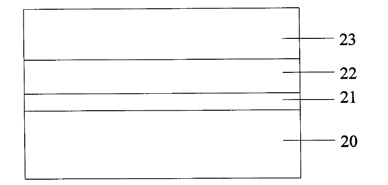
[0028] Step S200: forming a first insulating layer on the semiconductor substrate;

[0029] Step S300: forming a polysilicon layer on the insulating layer;

[0030] Step S400: forming a second insulating layer on the polysilicon layer;

[0031] Step S500: forming a mask layer on the second insulating layer;

[0032] Step S600: pe...


PUM

PropertyMeasurementUnit
thicknessaaaaaaaaaa
thicknessaaaaaaaaaa
thicknessaaaaaaaaaa

Abstract

The invention provides a method for reducing polycrystalline silicon loss in a mask etching process, which is applied to the manufacture of a floating gate of a flash memory device. The method comprises the following steps: providing a semiconductor substrate; forming a first insulating layer on the semiconductor substrate; forming a polycrystalline silicon layer on the insulating layer; forming a second insulating layer on the polycrystalline silicon layer; forming a mask layer on the second insulating layer; and carrying out dry plasma etching for the mask layer and stopping forming a groove on the second insulating layer. The method for reducing the polycrystalline silicon loss in the mask etching process can effectively reduce the polycrystalline silicon loss in the mask etching process in the floating grate manufacturing technology of the flash memory device, so the manufactured flash memory device has good electric performance.

Description

technical field [0001] The invention is designed in the field of integrated circuit manufacturing, and particularly relates to a method for reducing polysilicon loss in mask etching process. Background technique [0002] Flash memory has become a research hotspot in non-volatile memory due to its convenience, high storage density, and good reliability. Since the first flash memory product came out in the 1980s, with the development of technology and the storage needs of various electronic products, flash memory has been widely used in mobile and communication devices such as mobile phones, notebooks, handheld computers and U disks. , flash memory is a kind of non-volatile memory. Its operating principle is to control the switch of the gate channel by changing the critical voltage of the transistor or memory cell to achieve the purpose of storing data, so that the data stored in the memory will not be lost due to power interruption. Disappears, and flash memory is a special ...

Claims


Application Information

Patent Timeline
Patent Type & Authority Patents(China)
IPC IPC(8): H01L21/28H01L21/31H01L21/311H01L21/8247
Inventor 董耀旗孔蔚然
Owner SHANGHAI HUAHONG GRACE SEMICON MFG CORP
Features
  • R&D
  • Intellectual Property
  • Life Sciences
  • Materials
  • Tech Scout
  • Unparalleled Data Quality
  • Higher Quality Content
  • 60% Fewer Hallucinations
Learn More