Eureka AIR delivers breakthrough ideas for toughest innovation challenges, trusted by R&D personnel around the world.

Packaging structure for miniature electric field sensor and packaging method

A technology of electric field sensor and packaging structure, which is applied in the direction of microstructure device, processing microstructure device, microstructure technology, etc. It can solve the problems of electric leakage, shielding, and inability to measure, so as to achieve the effect of enhancing reliability and meeting application requirements

Active Publication Date: 2012-05-02
INST OF ELECTRONICS CHINESE ACAD OF SCI
View PDF0 Cites 0 Cited by
  • Summary
  • Abstract
  • Description
  • Claims
  • Application Information

AI Technical Summary

Problems solved by technology

[0006] The main problems that cause the miniature electric field sensor packaging technology to be solved so far, and cannot carry out accurate, long-term and reliable near-ground and airborne atmospheric electric field detection include: (1) The sensor packaging structure itself is charged, which affects the output of the sensor, and there are uncertain bias and Noise; (2) The noise generated by ion currents and temperature changes in the atmospheric environment makes measurement difficult; (3) The electrical leakage problem existing in the package cover and other package structures that introduce the measured electric field may lead to the shielding of the measured electric field, Unable to measure

Method used


Image

  • Packaging structure for miniature electric field sensor and packaging method
  • Packaging structure for miniature electric field sensor and packaging method
  • Packaging structure for miniature electric field sensor and packaging method

Examples


Embodiment Construction

[0021] Embodiments of the present invention will be specifically described below in conjunction with the accompanying drawings.

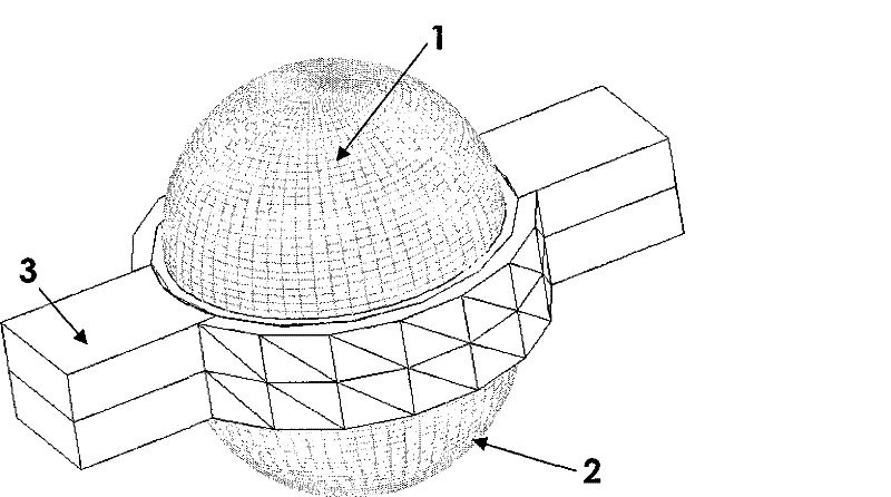
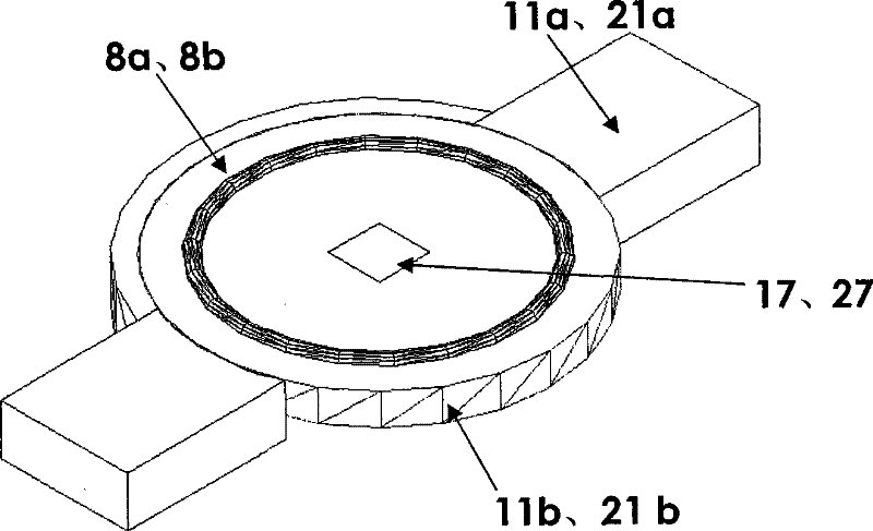
[0022] See figure 1 , the overall schematic diagram of the packaging structure of the miniature electric field sensor described in the present invention, figure 1 It is a three-dimensional view of the sensor package structure. this invention figure 1 The micro-electric field sensor packaging structure mainly includes: a first detection unit 1, a second detection unit 2 and two packaging support structures 3, and the first detection unit 1 and the second detection unit 2 are symmetrically placed between the two packaging support structures 3 inside, and fixedly connected with the packaging support structure 3 .

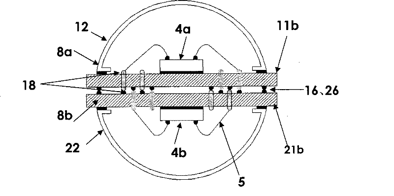
[0023] See figure 2 , showing the schematic structure of the first detection unit 1 and the second detection unit 2 and Figure 3A ,in:

[0024] The first detection unit 1 mainly includes a first sensor chip 4a, a first O-ring 8a, a f...


PUM


Abstract

The invention relates to a packaging structure for a miniature electric field sensor, which is capable of realizing static accumulation resistance, eliminating effects of self electrification and the like, and improving the reliability and stability of actual detection. The packaging structure for the miniature electric field sensor mainly comprises two same detection units and a packaging supporting structure, wherein each detection unit mainly comprises a substrate, a conductor cover, a sensor chip and the like, the sensor is arranged on the substrates respectively, and performs metal deposition and cablings to prepare a detection circuit of the sensor so as to realize close combination of the substrates and the conductive covers through the simple and efficient sealing technology. The detection units realize symmetric arrangement of the structure through the flip chip technology, and fix and mount the whole packaging structure by using the supporting structures packaged by the sensor. The packaging structure can realize system-in-package of the miniature electric field sensor.

Description

technical field [0001] The invention relates to a packaging structure of a miniature electric field sensor based on micromachining technology. Background technique [0002] The atmospheric electric field on the ground and in the air has gradually become an indispensable and important parameter in the fields of lightning warning and meteorological monitoring, and has important military significance and huge economic benefits. With the help of electric field sensors to monitor the changes of near-ground and air atmospheric electrostatic fields, accurate meteorological information can be obtained, thereby providing important safety guarantees for the launch of missiles, rockets, and satellites, as well as major disaster predictions such as earthquakes. In addition, electric field sensors also have important application requirements in the fields of industrial production, electric power and scientific research. [0003] Micro-electric field sensors based on micromachining techn...

Claims


Application Information

Patent Timeline
Patent Type & Authority Patents(China)
IPC IPC(8): B81B7/00B81C3/00
Inventor 彭春荣夏善红
Owner INST OF ELECTRONICS CHINESE ACAD OF SCI
Why Eureka
Eureka Blog
Learn More