

Method for optimizing integrated circuit of analog operational amplifier
An integrated circuit and analog computing technology, applied in the fields of instruments, computing, genetic models, etc., can solve problems such as being unsuitable for obtaining multi-parameter and multi-objectives, unable to obtain design parameters, and easy to fall into local optimum.
- Summary
- Abstract
- Description
- Claims
- Application Information
AI Technical Summary
Problems solved by technology
Method used
Image

Examples
Embodiment Construction
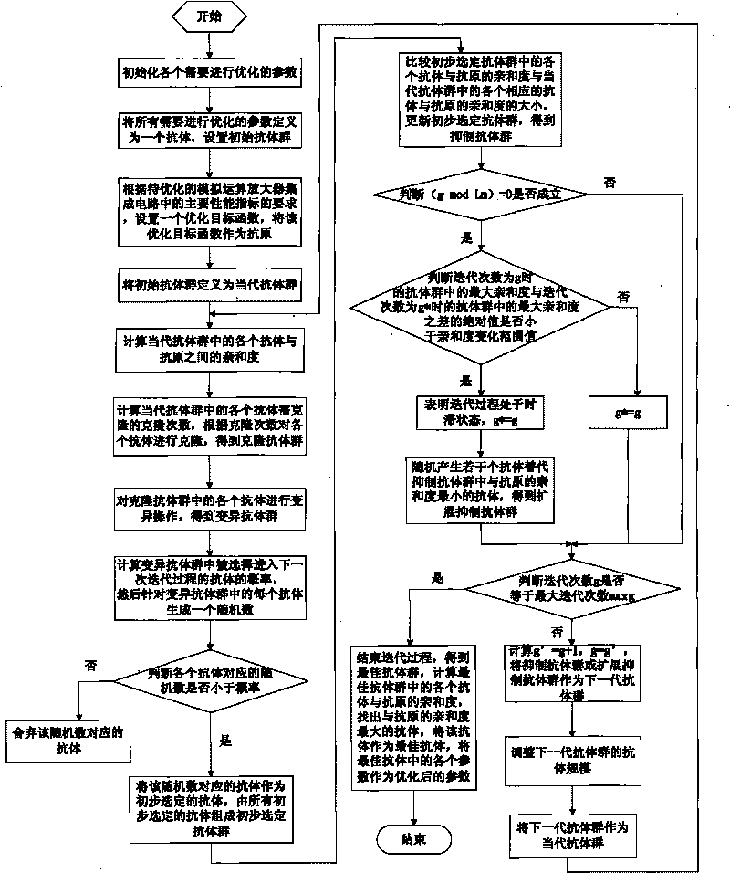
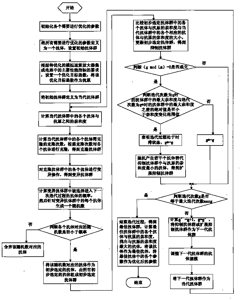
[0036] The present invention will be further described in detail below in conjunction with the accompanying drawings and embodiments.
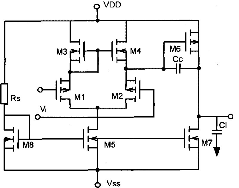
[0037] figure 1 A two-stage CMOS analog operational amplifier integrated circuit with eight tubes is given, where M1~M8 represent eight MOS (Metal Oxide Semiconductor, semiconductor metal oxide) tubes, the process parameters of M1 and M2 are the same, and the process parameters of M3 and M4 same. M1 and M2 form a P-channel transistor input-stage differential amplifier; N-channel transistors M3 and M4 form a basic constant current source as an active load for M1 and M2; M5 is a current source tube, which is a first-stage amplifier; N-channel tube M7 It is a common-source inverting amplifier tube, which is the second-stage amplifier, as the output stage; M6 is its active load; Rs and M8 form a bias circuit to provide operating current for the input-stage differential amplifier and output stage; V DD Indicates the forward supply voltage of the ...
PUM
 Abstract
Description
Claims
Application Information