
Isolated high-light load efficiency low-output voltage high-current switch power source
A low output voltage, high current switching technology, applied in the direction of converting DC power input to DC power output, output power conversion devices, electrical components, etc., can solve problems such as high cost and complex peripheral circuits, and achieve low cost and reliability. Good performance, the effect of preventing voltage spikes
- Summary
- Abstract
- Description
- Claims
- Application Information
AI Technical Summary
Problems solved by technology
Method used
Image

Examples
Embodiment Construction
[0021] Below in conjunction with accompanying drawing, the technical scheme of invention is described in detail:
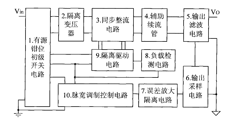
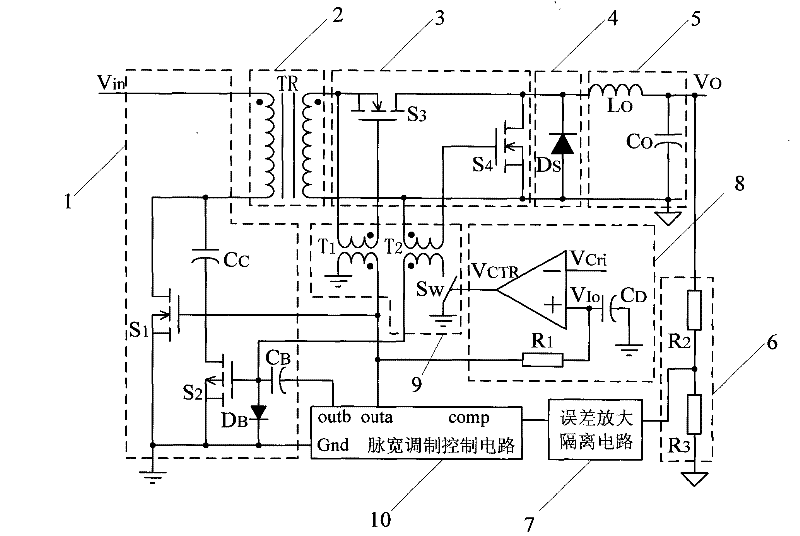
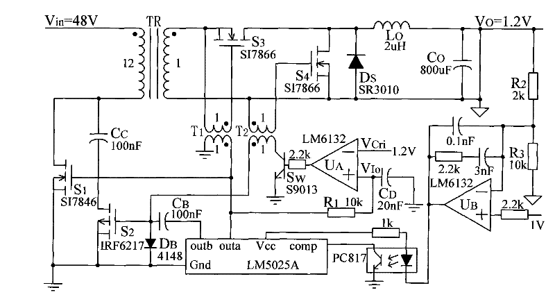
[0022] Such as figure 1 As shown, an isolated low output voltage high current switching power supply with high light load efficiency includes active clamp primary switching circuit 1, isolation transformer 2, synchronous rectification circuit 3, output filter circuit 5, output sampling circuit 6, error Amplify the isolation circuit 7 and the pulse width modulation control circuit 10, wherein the active clamp primary switch circuit 1 is sequentially connected in series with the isolation transformer 2 and the synchronous rectification circuit 3, and the active clamp primary switch circuit 1 is sequentially connected in series with the pulse width modulation control circuit 10 , error amplification isolation circuit 7, output sampling circuit 6 and output filter circuit 5, active clamp primary switch circuit 1 and pulse width modulation control circuit 10 are common...
PUM
 Abstract
Description
Claims
Application Information