Hetero-junction silicon solar cell and fabrication method thereof

A technology of silicon solar cells and manufacturing methods, applied in the direction of final product manufacturing, sustainable manufacturing/processing, circuits, etc., can solve the problems of high manufacturing cost, low efficiency, long manufacturing time, etc., and achieve fast processing time and low manufacturing cost. , the effect of high short-circuit current

Inactive Publication Date: 2010-09-01
LG ELECTRONICS INC
View PDF0 Cites 4 Cited by
  • Summary
  • Abstract
  • Description
  • Claims
  • Application Information

AI Technical Summary

Problems solved by technology

[0009] However, in heterojunction silicon solar cells, compared to the reference figure 1 Described amorphous / crystalline pn heterojunction silicon solar cells in which a p-type amorphous silicon layer is deposited on an n-type crystalline silicon substrate compared to a solar cell in which an n-type amorphous silicon layer is deposited on a p-type crystalline silicon substrate The structure of amorphous / crystalline np heterojunction silicon solar cells has the problem of low efficiency
In addition, since the fabrication of amorphous / crystalline heterojunction solar silicon cells requires many vacuum deposition devices compared with the fabrication of conventional diffused crystalline silicon solar cells, there are problems of long manufacturing time and high manufacturing costs

Method used


Image

  • Hetero-junction silicon solar cell and fabrication method thereof
  • Hetero-junction silicon solar cell and fabrication method thereof
  • Hetero-junction silicon solar cell and fabrication method thereof

Examples


Embodiment Construction

[0039] Hereinafter, preferred embodiments of the present invention will be described in detail with reference to the accompanying drawings.

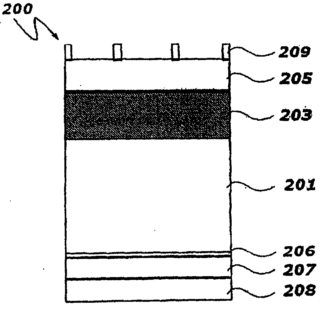
[0040] figure 2 is a cross-sectional view schematically showing the structure of a heterojunction silicon solar cell according to one embodiment of the present invention.

[0041] like figure 2 As shown, the heterojunction silicon solar cell 200 of the present invention includes a p-type crystalline silicon substrate 201, on which a passivation layer 203, an anti-reflection layer 205, and an upper electrode 209 are sequentially formed. A textured structure 206, a field forming layer (BSF) 207, and a lower electrode 208 are sequentially formed.

[0042] The heterojunction silicon solar cell 200 is an amorphous / crystalline np heterojunction structure and includes a passivation layer 203 deposited on a p-type crystalline silicon substrate 201 serving as an n-type amorphous silicon layer. Meanwhile, the heterojunction silicon solar cell...


PUM


Abstract

Disclosed are a hetero-junction silicon solar cell and a fabrication method thereof. The hetero-junction silicon solar cell according to the present invention forms a pn junction of a crystalline silicon substrate and a passivation layer doped with impurities so as to minimize a recombination of electrons and holes, making it possible to maximize efficiency of the hetero-junction silicon solar cell. The present invention provides a hetero-junction silicon solar cell comprising a crystalline silicon substrate and a passivation layer that is formed on the crystalline silicon substrate and is doped with impurities.

Description

technical field [0001] The invention relates to a heterojunction silicon solar cell and a manufacturing method thereof. More specifically, the present invention relates to a heterojunction silicon solar cell and a manufacturing method thereof that form a pn junction of a crystalline silicon substrate and a passivation layer doped with impurities so as to minimize recombination of electrons and holes, Maximizing the efficiency of heterojunction silicon solar cells. Background technique [0002] In recent years, new forms of renewable energy have received much attention due to issues such as rising oil prices, global warming, depletion of fossil energy sources, nuclear waste disposal, site selection involved in construction of new power plants, and the like. Among them, research and development of solar cells as non-polluting energy sources have been actively promoted. [0003] Solar cells, which are devices that convert light energy into electrical energy using the photoele...

Claims


Application Information

Patent Timeline
Patent Type & Authority Applications(China)
IPC IPC(8): H01L31/042
CPCH01L31/18H01L31/1804H01L31/0745H01L31/022425Y02E10/547H01L31/0747Y02P70/50H01L31/04H01L31/072
Inventor 高志勋鱼英株金真阿尹周焕郑一炯金钟焕
Owner LG ELECTRONICS INC
Why Eureka
Try Eureka