
GGNMOS device used in ESD protective circuit

A technology of ESD protection and devices, which is applied in the direction of circuits, electrical components, semiconductor devices, etc., can solve problems such as the difficulty of leakage of electrostatic current, the increase of trigger voltage, and the reduction of leakage channel resistance

Active Publication Date: 2015-01-07
SHANGHAI HUAHONG GRACE SEMICON MFG CORP
View PDF3 Cites 0 Cited by
  • Summary
  • Abstract
  • Description
  • Claims
  • Application Information

AI Technical Summary

Problems solved by technology

[0010] The present invention solves the problem of non-uniform triggering of GGNMOS devices used for ESD protection in the prior art, and solves the problems of reduced resistance in the leakage channel, increased trigger voltage, and difficult leakage of electrostatic current

Method used


Image

  • GGNMOS device used in ESD protective circuit
  • GGNMOS device used in ESD protective circuit
  • GGNMOS device used in ESD protective circuit

Examples


Embodiment Construction

[0024] In order to make the content of the present invention clearer and easier to understand, the novel content of the present invention will be further described below in conjunction with the accompanying drawings. Of course, the present invention is not limited to this specific embodiment, and general replacements known to those skilled in the art are also covered within the protection scope of the present invention.

[0025] Secondly, the present invention is described in detail by means of schematic diagrams. When describing the examples of the present invention in detail, for the convenience of explanation, the schematic diagrams are not partially enlarged according to the general scale, which should not be used as a limitation of the present invention.
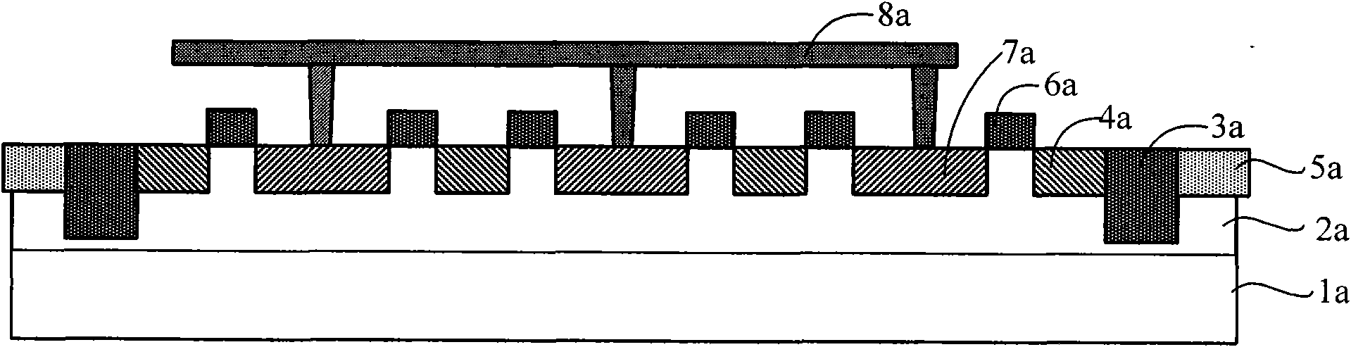
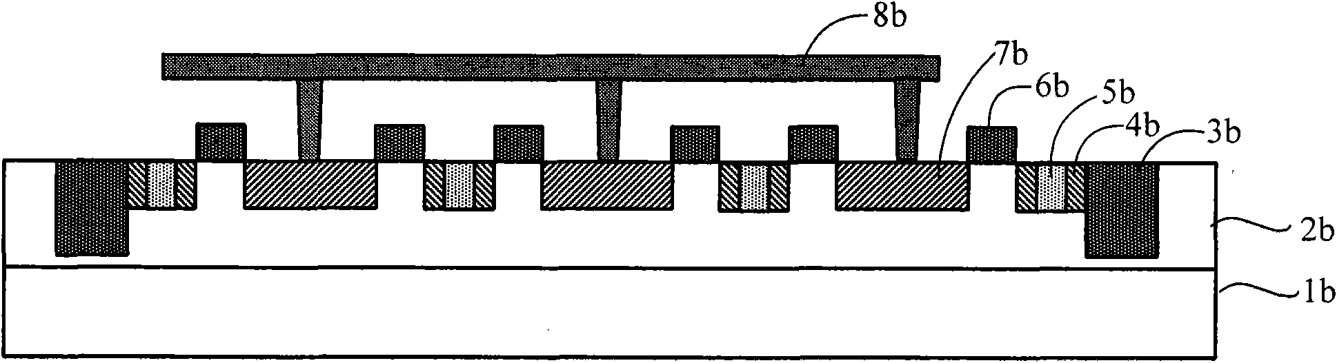
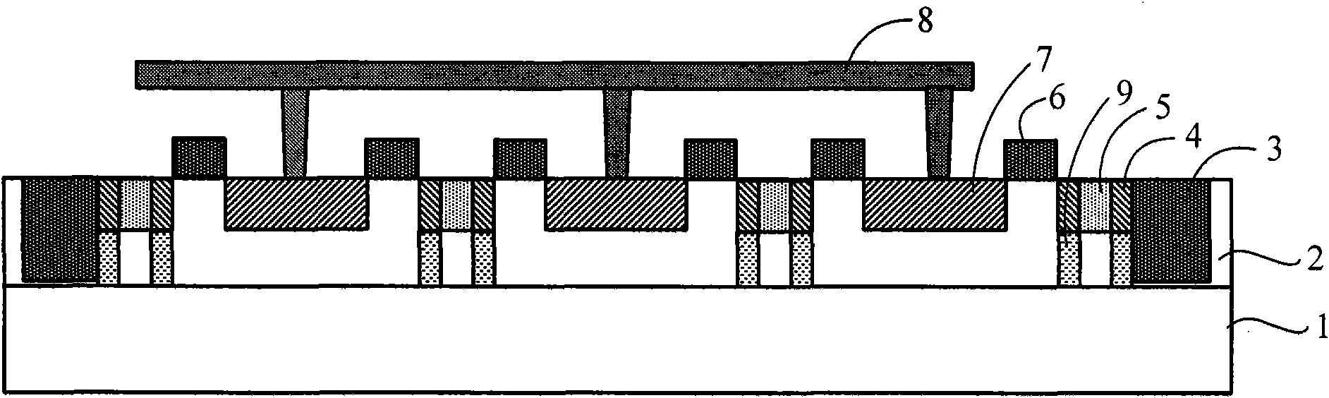
[0026] The central idea of ​​the present invention is that setting a P-type doped region between the source regions can solve the uniformity problem, and at the same time, setting an N well region directly below the sour...


PUM


Abstract

The invention provides a GGNMOS device used in an ESD protective circuit. The device comprises a substrate and a P trap region positioned on the substrate, wherein a plurality of drain electrode regions are arranged in the P trap region; the surface of the P trap region and two sides of the drain electrode regions are provided with grid electrode regions; the P trap region and the other sides of the grid electrode regions are provided with source electrode regions; P type doped regions are arranged among the source electrode regions; and a position below the source electrode regions and close to the source electrode regions is provided with an N trap region. The GGNMOS device used in the ESD protective circuit not only can solve non-uniform triggering problems, but also can solve the problems of resistance reduction, trigger voltage raising and difficult leakage of electrostatic current in a leakage path.

Description

technical field [0001] The invention relates to an ESD protection circuit, in particular to a GGNMOS device used for the ESD protection circuit. Background technique [0002] In integrated circuit IC chip manufacturing and final application systems, with the continuous improvement of VLSI process technology, CMOS integrated circuits have entered the ultra-deep sub-micron stage, the size of MOS devices is continuously shrinking, and the thickness of the gate oxide layer is increasing The thinner the gate is, the lower its gate withstand voltage capability is, and the harm of electrostatic discharge (Electrostatic Discharge, ESD) to integrated circuits becomes more and more significant. According to statistics, 35% of products with integrated circuit failures are caused by ESD problems. Therefore, it is particularly important to design ESD protection for integrated circuits. [0003] The ESD protection circuit is a discharge path that provides electrostatic current for the c...

Claims


Application Information

Patent Timeline
Patent Type & Authority Patents(China)
IPC IPC(8): H01L27/088H01L29/78H01L29/06
Inventor 胡剑
Owner SHANGHAI HUAHONG GRACE SEMICON MFG CORP
Learn More