Supercharge Your Innovation With Domain-Expert AI Agents!

Hybrid packaged gate controlled semiconductor switching device and preparing method

A switching device and hybrid packaging technology, applied in the fields of semiconductor/solid-state device manufacturing, semiconductor devices, semiconductor/solid-state device components, etc., can solve problems such as aggravating the restriction effect and increasing the leakage current potential of the device.

Inactive Publication Date: 2011-04-06
ALPHA & OMEGA SEMICON INC
View PDF7 Cites 9 Cited by
  • Summary
  • Abstract
  • Description
  • Claims
  • Application Information

AI Technical Summary

Problems solved by technology

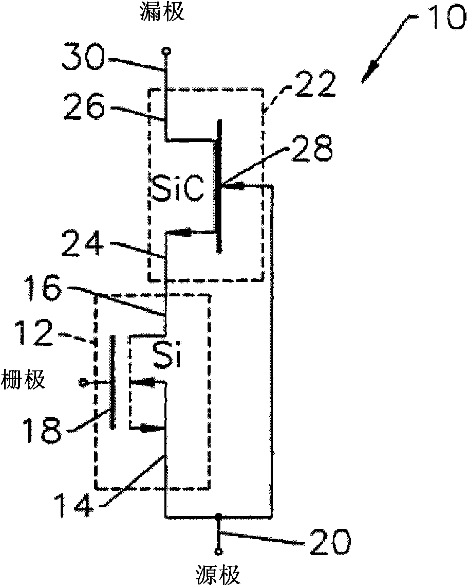
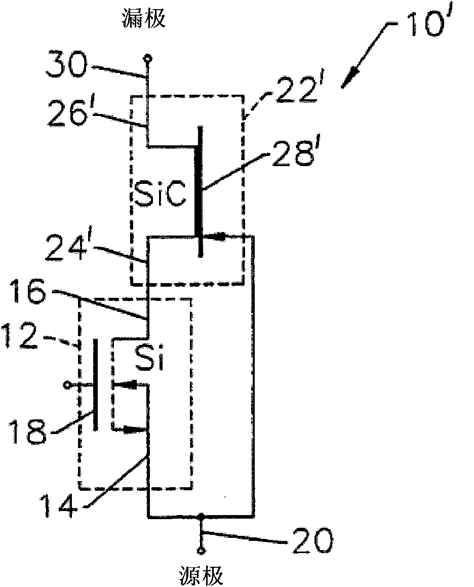
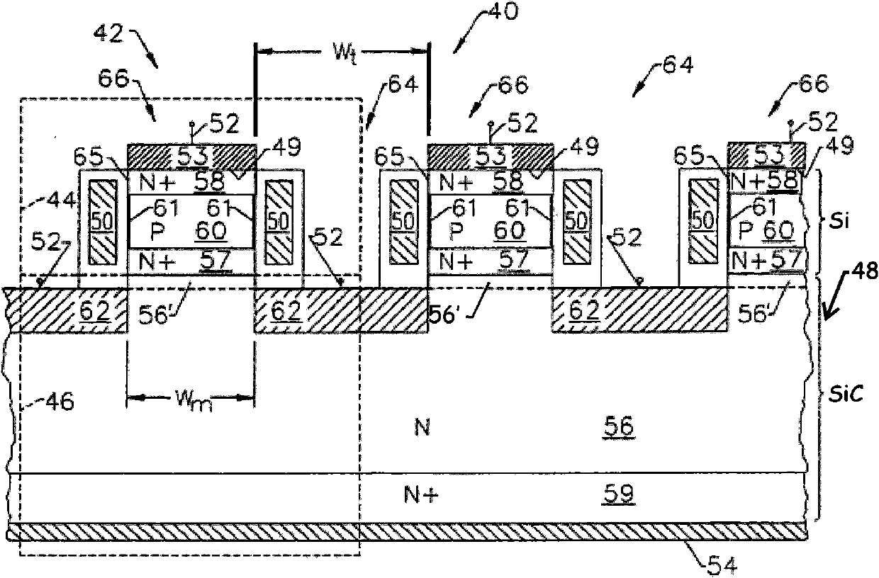
[0006] It is worth noting that with the mixed substrate of silicon and silicon carbide, the device structure flexibility of the switching devices 10 and 10' can be limited by the compatibility of materials and processes at the silicon-silicon carbide interface
This limitation is exacerbated by the overall tight package size of switching devices 10 and 10'
Another concern about silicon-silicon carbide substrates is the potential increase in device leakage due to molecular-level structural defects at the silicon-silicon carbide interface

Method used


Image

  • Hybrid packaged gate controlled semiconductor switching device and preparing method
  • Hybrid packaged gate controlled semiconductor switching device and preparing method
  • Hybrid packaged gate controlled semiconductor switching device and preparing method

Examples


Embodiment Construction

[0045] The description herein and the drawings are only intended to illustrate one or more presently preferred embodiments of the present invention, as well as some additional features and / or alternative embodiments. These descriptions and drawings are for illustration only and not as limitations of the present invention. Accordingly, variations, modifications, and alternatives will be within the grasp of those skilled in the art. These changes, modifications and alternatives should also be considered within the scope of the present invention.

[0046] image 3 and Figure 4A A perspective view showing a first device structure of a hybrid packaged 3-terminal gate controllable semiconductor switching device (HPSD) 50 with a rectifying gate transistor (RGT) wafer 10 according to the present invention.

[0047] The HPSD 50 has a package base in which various leadframe sections 30a, 30b, 30c and 30d are contained. Each lead frame section 30b, 30c and 30d has a plurality of pac...


PUM


Abstract

A hybrid packaged gate controlled semiconductor switching device (HPSD) has an insulated-gate transistor (IGT) made of a first semiconductor die and a rectifying-gate transistor (RGT) made of a second semiconductor die. The RGT gate and source are electrically connected to the IGT source and drain respectively. The HPSD includes a package base with package terminals for interconnecting the HPSD to external environment. The IGT is die bonded atop the package base. The second semiconductor die is formed upon a composite semiconductor epi layer overlaying an electrically insulating substrate (EIS) thus creating a RGT die. The RGT die is stacked and bonded atop the IGT die via the EIS. The IGT, RGT die and package terminals are interconnected with bonding wires. Thus, the HPSD is a stacked package of IGT die and RGT die with reduced package footprint while allowing flexible placements of device terminal electrodes on the IGT.

Description

technical field [0001] The present invention generally relates to the field of circuits. More specifically, the present invention relates to physical level packaging and fabrication methods for electronic switching circuits. Background technique [0002] In addition to technically sound schematic circuit design, today's electronics require high-quality, efficient physical-level packaging. Especially in portable product applications, tight package size, low electromagnetic interference / radio frequency interference (EMI / RFI) and flexibility of system structure are extremely important considerations. [0003] U.S. Patent No. US5396085 invented by Baliga et al. entitled "Silicon carbide switching device with rectifying gate", hereinafter cited as US5396085, proposes a silicon carbide switching device on a mixed substrate of silicon and silicon carbide Among them, a three-terminal interconnected silicon MOSFET and a silicon carbide MESFET (or JFET) are included. For simplicity...

Claims


Application Information

Patent Timeline
Patent Type & Authority Applications(China)
IPC IPC(8): H01L25/065H01L21/98
CPCH01L2924/30107H01L25/50H01L2224/48247H01L2924/13091H01L2224/48091H01L2224/48245H01L2224/48145H01L24/48H01L2224/49111H03K17/567H01L23/49575H01L2924/13062H01L2924/13063H01L2924/14H01L2924/00014H01L24/49H01L2224/0603H01L2224/48257H01L2924/00H01L2224/45099H01L2224/45015H01L2924/207H01L2924/00012
Inventor 雷燮光安荷·叭剌
Owner ALPHA & OMEGA SEMICON INC
Features
  • R&D
  • Intellectual Property
  • Life Sciences
  • Materials
  • Tech Scout
  • Unparalleled Data Quality
  • Higher Quality Content
  • 60% Fewer Hallucinations
Learn More