Display panel

A display panel and display area technology, applied in nonlinear optics, instruments, optics, etc., can solve problems such as component impact damage, circuit scratches on the substrate surface, etc., to strengthen the restraint effect, improve test yield and test accuracy Effect

Inactive Publication Date: 2011-07-13
AU OPTRONICS CORP
View PDF6 Cites 10 Cited by
  • Summary
  • Abstract
  • Description
  • Claims
  • Application Information

AI Technical Summary

Problems solved by technology

However, limited to the existing test pad structure, when the probe is in contact with the test pad, it is easy to make the probe slide and deflect on the surface of the test pad a

Method used


Image

  • Display panel
  • Display panel
  • Display panel

Examples


Embodiment Construction

[0033] The display panel of the present invention may be a liquid crystal display panel, an organic electroluminescence panel, and other types of display panels that display frame images through pixel arrays. The following will take a liquid crystal display panel as an example to illustrate the actual structure of applying the test pad design of the present invention to it.

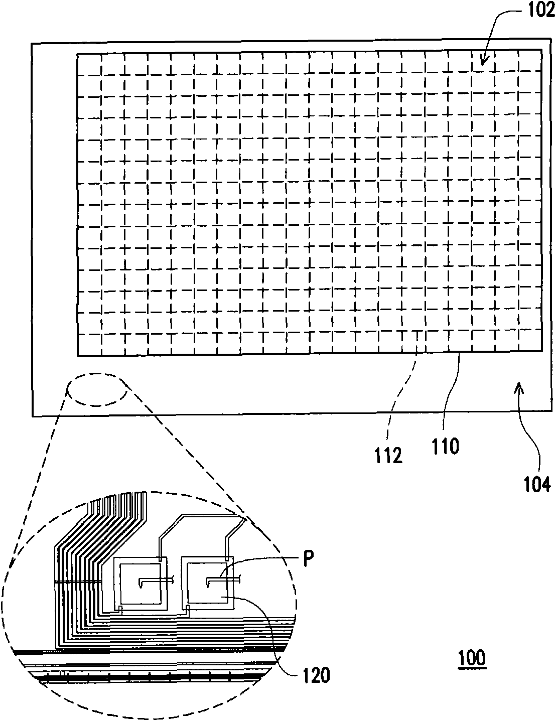
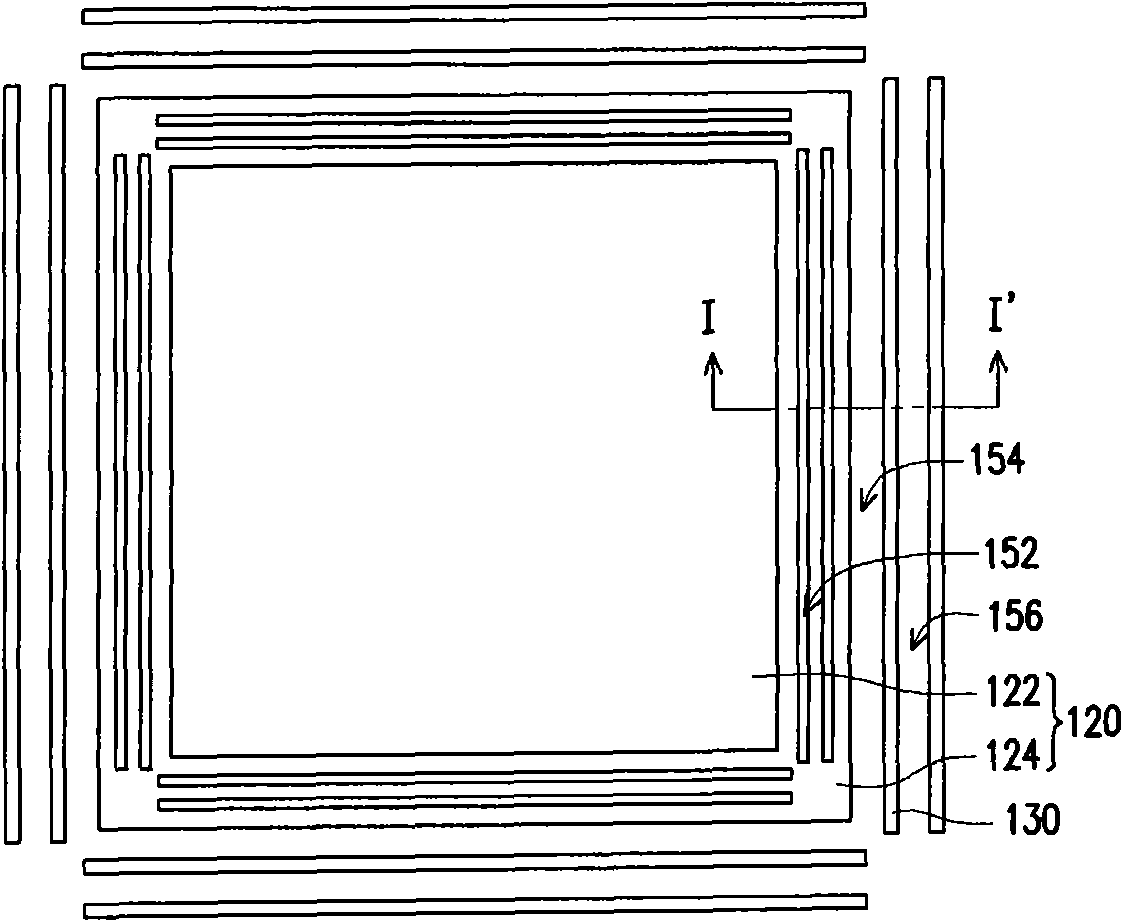
[0034] figure 1 It is a schematic diagram of a liquid crystal display panel and a partially enlarged view thereof according to an embodiment of the present invention. Such as figure 1 As shown, the liquid crystal display panel 100 has a display area 102 and a peripheral circuit area 104 located on the periphery of the display area 102 . The display area 102 has a pixel array 110 composed of a plurality of pixel units 112 , and the peripheral line area 104 has one or more test pads 120 electrically connected to the pixel array 110 .

[0035] Generally speaking, the liquid crystal display panel 100 is co...


PUM


Abstract

The invention provides a display panel, comprising a substrate, a pixel array, and a test pad. The substrate is provided with a support surface, a display district, and a circumferential line district at the periphery of the display district. The pixel array is disposed on the support surface and located in the display district. The test pad is disposed on the support surface and located in the circumferential line district. The test pad is electrically connected with the pixel array. The test pad comprises a central part and a peripheral part surrounding the central part, wherein the height of the peripheral part is greater than the height of the central part, and the peripheral part is provided with a plurality of first grooves. The first grooves are exposed out of the support surface.

Description

technical field [0001] The present invention relates to a display panel, and in particular to a display panel with test pads. Background technique [0002] Common display panels on the market today, such as liquid crystal display panels, can be divided into a display region and a peripheral circuit region. A plurality of pixel units arranged in an array are arranged in the display region to display frame screen. Drivers and test lines electrically connected to the pixel units are provided in the peripheral circuit area to drive the pixel units or perform electrical testing on the pixel units. Through electrical testing, it can be judged whether the pixel unit can operate normally. When the pixel unit fails to operate normally, defective elements (such as thin film transistors or pixel electrodes, etc.) or circuits can be repaired. [0003] The way of electrical testing is usually to touch the test pads of the test circuit with the probes to input test signals to each pixe...

Claims


Application Information

Patent Timeline
IPC IPC(8): G02F1/13G02F1/136
Inventor 陈柄霖廖一遂
Owner AU OPTRONICS CORP
Why Eureka
Try Eureka