Check patentability & draft patents in minutes with Patsnap Eureka AI!

TFT array substrate and LCD panel

A technology of thin film transistors and array substrates, applied in the field of liquid crystal displays, can solve problems such as picture quality degradation

Active Publication Date: 2012-12-26
HANNSTAR DISPLAY CORPORATION
View PDF0 Cites 0 Cited by
  • Summary
  • Abstract
  • Description
  • Claims
  • Application Information

AI Technical Summary

Problems solved by technology

Therefore, in the common line in the existing pixel matrix, the signal delay effect caused by its resistance and capacitance is quite obvious, which reduces the picture quality

Method used


Image

  • TFT array substrate and LCD panel
  • TFT array substrate and LCD panel
  • TFT array substrate and LCD panel

Examples


Embodiment Construction

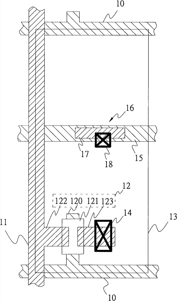
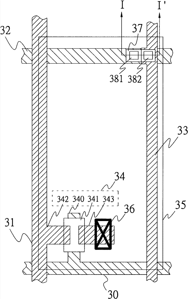
[0071] image 3 It is a schematic layout diagram of a pixel structure according to an embodiment of the present invention, Figure 4 Then it is a schematic cross-sectional view along the section line I-I'.

[0072] see image 3 , The pixel electrode structure includes: a gate line 30 , a data line 31 , a first common line 32 , a second common line 33 and a thin film transistor 34 . The gate lines 30 are arranged along a first direction, and the data lines 31 are arranged along a second direction, and the second direction is substantially perpendicular to the first direction. The first common line 32 is parallel to the gate line 30 , and the second common line 33 crosses the gate line 30 . The thin film transistor 34 includes: a gate 340 , a channel layer 341 , a source 342 and a drain 343 . The gate 340 is electrically connected to the gate line 30 , the source 342 is electrically connected to the data line 31 , and the drain 343 is electrically connected to the pixel elec...


PUM


Abstract

A TFT array substrate includes gate lines, data lines, and first and second common lines. The gate lines are disposed on a transparent substrate. The data lines cross the gate lines. There is no pixel region defined by adjacent two of gate lines and adjacent two of the data lines. There are two pixel regions being left and right pixel region defined by adjacent two of gate lines and adjacent two of the data lines. The first common lines are parallel to the gate lines. The second common lines are parallel to the data lines and electrically connected to the first common lines, wherein each second common line is disposed between the left and right pixel regions.

Description

technical field [0001] The present invention provides a liquid crystal display, especially a thin film transistor array substrate of a liquid crystal panel of a liquid crystal display, which has a common line of mesh structure to reduce the signal delay effect caused by resistance and capacitance. Background technique [0002] Generally speaking, a Liquid Crystal Display (LCD) can display image data by separately providing data signals corresponding to the image data to liquid crystal cells (Liquid Crystal Cells) and adjusting light transmittance of the liquid crystal cells. The liquid crystal display includes: a liquid crystal panel with liquid crystal cells arranged in a matrix, and an integrated circuit (Integrated Circuit, IC) for driving. [0003] The liquid crystal panel also includes: a color filter substrate; a thin film transistor array substrate corresponding to the color filter substrate; and a liquid crystal layer sandwiched between the color filter substrate and...

Claims


Application Information

Patent Timeline
Patent Type & Authority Patents(China)
IPC IPC(8): H01L27/02H01L23/528H01L21/77H01L21/768G02F1/1362G02F1/1368G02F1/1333
Inventor 蔡瑞鑫游家华李昆政
Owner HANNSTAR DISPLAY CORPORATION
Features
  • R&D
  • Intellectual Property
  • Life Sciences
  • Materials
  • Tech Scout
  • Unparalleled Data Quality
  • Higher Quality Content
  • 60% Fewer Hallucinations
Learn More