Sensitive element device for bypass signal of sensing circuit and detection method of sensitive element device
A technology of bypass signal and induction circuit, applied in the field of sensitive element device and its detection, can solve the problems of large human error and high consumption, and achieve the effect of stable characteristic value and saving labor and material resources.
- Summary
- Abstract
- Description
- Claims
- Application Information
AI Technical Summary
Problems solved by technology
Method used
Image
Examples
Embodiment
[0033] The technical solution of the present invention will be further specifically described below in conjunction with the accompanying drawings.
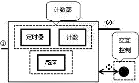
[0034] figure 1 The overall design framework is given, the right side is a brief description of the port, and the design diagram on the left mainly includes four parts: counting part, interactive control part, port part and sensing part.
[0035] figure 1 Among them, ①Enabling the control terminal can stop the entire HTD-PUF from working and isolate it from the original circuit. ②Data output, this port is a vector port, the number of bits is determined according to the characteristics of the sensor. ③Probe port, the port for interacting with the original circuit.
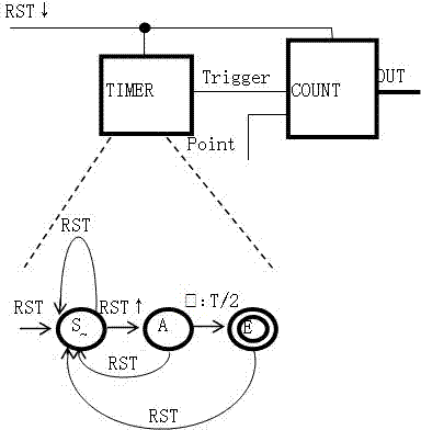
[0036] figure 2 TIMER (timer) and COUNT (counter) are controlled by the same RST (reset signal). Point is the counting basis port of COUNT, that is, the number of signal transitions at the Point port is calculated. The operation process is as follows:
[0037] ...
PUM
 Abstract
Description
Claims
Application Information


