
An integrated circuit with high overload resistance

An integrated circuit and high-resistance technology, applied in the field of assembly structure, can solve the problems of low level of substrate high-resistance overload, and hybrid integrated circuit substrate is easy to fall off. sexual effect

Active Publication Date: 2015-07-29
EAST CHINA INST OF OPTOELECTRONICS INTEGRATEDDEVICE
View PDF4 Cites 0 Cited by
  • Summary
  • Abstract
  • Description
  • Claims
  • Application Information

AI Technical Summary

Problems solved by technology

[0003] The purpose of the present invention is to solve the problem that the hybrid integrated circuit substrate is easy to fall off under the impact of high overload, and the substrate has a low level of high overload resistance, and provides a high overload resistant integrated circuit

Method used


Image

  • An integrated circuit with high overload resistance
  • An integrated circuit with high overload resistance
  • An integrated circuit with high overload resistance

Examples


Embodiment Construction

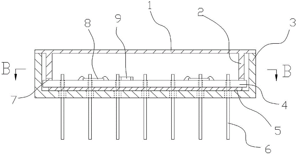
[0013] Such as figure 1 As shown, a high overload resistant integrated circuit provided by the present invention includes a housing 3, the bottom surface of the housing 3 is assembled with a substrate 4 through insulating glue (or other assembly materials, such as solder, etc.) 5, and a chip 8, For circuit components such as the device 9, the substrate 4 is provided with electrodes 6 passing through the bottom surface of the casing. A sealing cover 1 is provided at the upper end of the housing, and a support 2 is provided on the side of the sealing cover extending toward the inner cavity of the housing, and the support 2 forms a pressing and positioning fit with the substrate. An insulating glue 7 is provided between the bottom surface of the support member 2 and the substrate to be in contact, and the support structure and the substrate can be effectively bonded by curing.

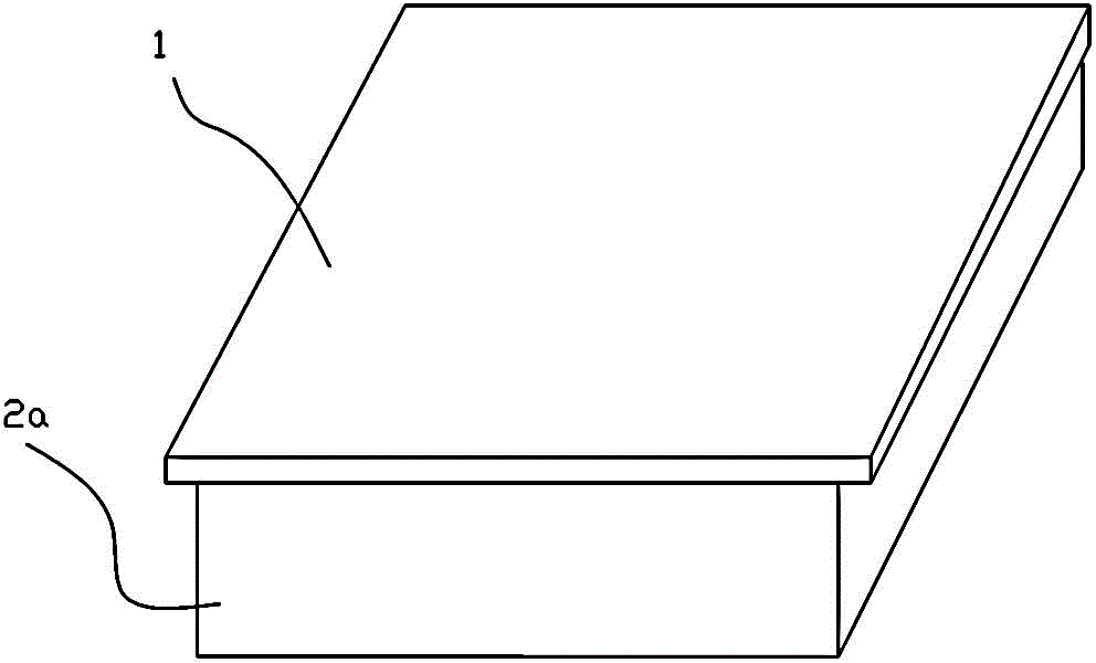
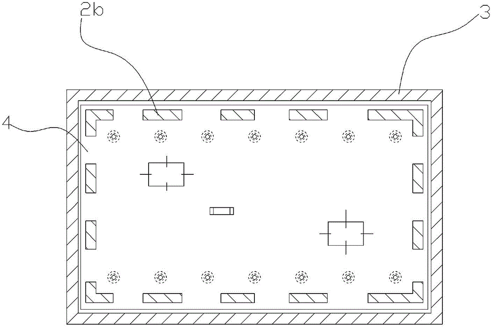
[0014] Such as figure 2 As shown, the supporting member can be a rectangular frame 2a arranged on o...


PUM


Abstract

The invention relates to an anti-high-overload integrated circuit in a micro electronic product. The anti-high-overload integrated circuit comprises a casing (3), wherein a substrate (4) is connected to the interior of the casing (3); and a sealing cover (1) is arranged at the upper end of the casing. The anti-high-overload integrated circuit is characterized in that a support piece (2) is arranged on one side of the sealing cover, and the support piece (2) is matched with the substrate in a compressing and positioning manner. The anti-high-overload integrated circuit has the advantages that a mature substrate and casing assembly method of a hybrid integrated circuit is better carried on, and meanwhile, a concise substrate support and protection method is provided, so that the anti-high-overload level of both the substrate and the product is remarkably improved, and strong practicability is realized.

Description

technical field [0001] The invention relates to the field of electronic product manufacturing, in particular to an assembly structure between a substrate and a metal casing in a microelectronic product. Background technique [0002] The high overload resistance performance of microelectronic products refers to the ability of the product itself to resist high-intensity mechanical impact. Since there are many components assembled on the surface of the hybrid integrated circuit substrate, compared with a single component, the overall weight of the substrate and the components on it is much larger, and the impact inertia force it bears during the overload shock process is also greater. At the same time, the substrate of the conventional hybrid integrated circuit is directly assembled on the inner bottom surface of the metal shell substrate, and the substrate does not have any supporting structure in the Y1 direction. The weak link of the hybrid integrated circuit to withstand h...

Claims


Application Information

Patent Timeline
Patent Type & Authority Patents(China)
IPC IPC(8): H01L23/04
Inventor 夏俊生张静
Owner EAST CHINA INST OF OPTOELECTRONICS INTEGRATEDDEVICE
Learn More