Shift register, grid driving circuit and display device

A shift register and gate connection technology, applied in the field of gate drive circuits, display devices, and shift registers, can solve the problem that the shift register cannot realize bidirectional scanning, and achieve the effect of overcoming reverse scanning.

Active Publication Date: 2013-02-27
BOE TECH GRP CO LTD +1
View PDF4 Cites 64 Cited by
  • Summary
  • Abstract
  • Description
  • Claims
  • Application Information

AI Technical Summary

Benefits of technology

This patented technology allows for two different modes of operation: one mode called normal scans where both directions can be controlled by an upward or downward movement (forward/back) button while another mode called backscattering involves controlling only certain parts of the image being displayed without actually shifting them around during display time. By doing this, it becomes possible to achieve full duplex displays with improved resolution compared to traditional methods like rasterization techniques.

Problems solved by technology

This patented technical problem addressed in this patents relates to improving the performance of thin film transistor liquid crystal displays (TFT LCDs) with shifting registers due to their high costs associated therewith. Current designs require two stages for each stage, which means they have limitations such as requiring twice or more time during fabrication processes compared to single level CMOS circuits.

Method used


Image

  • Shift register, grid driving circuit and display device
  • Shift register, grid driving circuit and display device
  • Shift register, grid driving circuit and display device

Examples


Embodiment 1

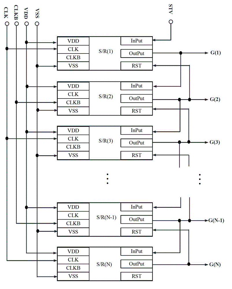
[0033] like image 3 As shown, it is a schematic structural diagram of the shift register in Embodiment 1 of the present invention, wherein:

[0034] Except for the shift register unit of the first stage and the shift register unit of the Nth stage, the signal output terminal OutPut of the shift register unit S / R(n) of each stage is connected to the adjacent shift register unit S of the next stage. The first signal input terminal InPut1 of / R(n+1), the second signal input terminal InPut2 of the S / R(n+1), and the adjacent shift register unit S / R(n- 1) the first signal input terminal and the second signal input terminal of the S / R(n-1) are connected, and the n is a positive integer greater than 1 and less than N;

[0035] The frame start signal STV is respectively connected to the first signal input terminal of the first stage shift register unit and the second signal input terminal of the Nth stage shift register unit;

[0036] The forward scan signal and the reverse scan sig...

Embodiment 2

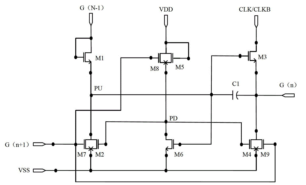
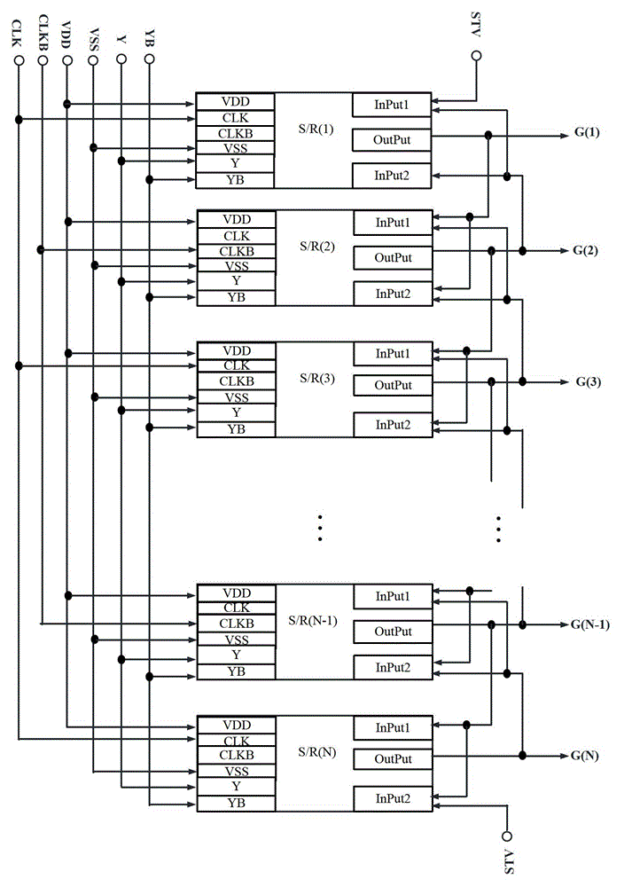
[0051] Embodiment two of the present invention is respectively to embodiment one Figure 4 and Figure 5 The specific circuit structure of the shift register unit is described in detail.

[0052] against Figure 4 The structure of the shift register unit shown, its specific circuit can be Image 6 As shown, among them,

[0053] Forward scan switch module 101 includes:

[0054] The tenth transistor M10 has its source connected to the first signal input terminal, its gate connected to the forward scanning signal input terminal, and its drain connected to the input node of the pull-up drive module;

[0055] The drain of the eleventh transistor M11 is connected to the second signal input terminal, the gate is connected to the forward scanning signal input terminal, and the source is connected to the input node of the second pull-down module.

[0056] The reverse scan switch module 102 includes:

[0057] The twelfth transistor has its drain connected to the second signal inpu...

Embodiment 3

[0113] In order to further illustrate the shift register unit provided in the second embodiment of the present invention, the third embodiment uses Figure 7 The circuit of the shift register unit shown as an example, combined with Figure 9 and Figure 10 The scan timing diagram shown illustrates how it works.

[0114] like Figure 9 As shown, it is a schematic diagram of the forward scanning timing of the shift register provided by Embodiment 3 of the present invention, wherein:

[0115] CLK is the clock signal of the input shift register unit S / R(n);

[0116] CLKB is the clock signal of input shift register unit S / R(n-1) and shift register unit S / R(n+1);

[0117] GOUT (n-1) is the signal output by the shift register unit S / R(n-1) of the upper stage of the shift register unit S / R(n), as the signal of the shift register unit S / R(n) of the current stage input signal;

[0118] YB is the positive scanning signal input to the shift register unit S / R(n), which is a high-leve...


PUM


Abstract

The invention discloses a shift register, a grid driving circuit and a display device. The shift register is mainly characterized in that the shift register forwardly outputs output signals of each stage of shift register unit through a signal output terminal of each stage of shift register unit according to forward scanning signals, and reversely outputs output signals of each stage of shift register unit through the signal output terminal of each stage of shift register unit according to reverse scanning signals; each stage of shift register unit comprises a forward scanning switch module used for connecting a pull-up driving module under the control of the forward scanning signals, outputting first signals to a pull-up node and outputting second signals to a second pull-down module, a reverse scanning switch module used for connecting the pull-up driving module under the control of the reverse scanning signals, outputting the second signals to the pull-up node and outputting the first signals to the second pull-down module, the pull-up driving module, a pull-up module, a pull-down driving module, a first pull-down module and the second pull-down module. The forward scanning switch module and the reverse scanning switch module are utilized to control different signals to be input into different modules, so that forward scanning can be realized.

Description


Claims


Application Information

Patent Timeline
Owner BOE TECH GRP CO LTD
Why Eureka
Try Eureka