A kind of shift register, its driving method and gate driving circuit

A shift register and gate technology, which is applied in the field of shift registers and gate drive circuits, can solve problems such as the design of narrow borders that are unfavorable for display panels.

Active Publication Date: 2018-02-16
BOE TECH GRP CO LTD +1
View PDF7 Cites 0 Cited by
  • Summary
  • Abstract
  • Description
  • Claims
  • Application Information

AI Technical Summary

Problems solved by technology

However, the existing shift registers can generally only realize one-way scanning. Although there are currently shift registers that can realize bidirectional scanning, they need special control signals to control the scanning direction, which requires additional wiring to provide control signals. Therefore, it is not conducive to the narrow frame design of the display panel.

Method used


Image

  • A kind of shift register, its driving method and gate driving circuit
  • A kind of shift register, its driving method and gate driving circuit
  • A kind of shift register, its driving method and gate driving circuit

Examples


example 1

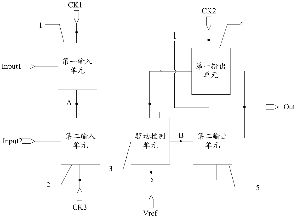
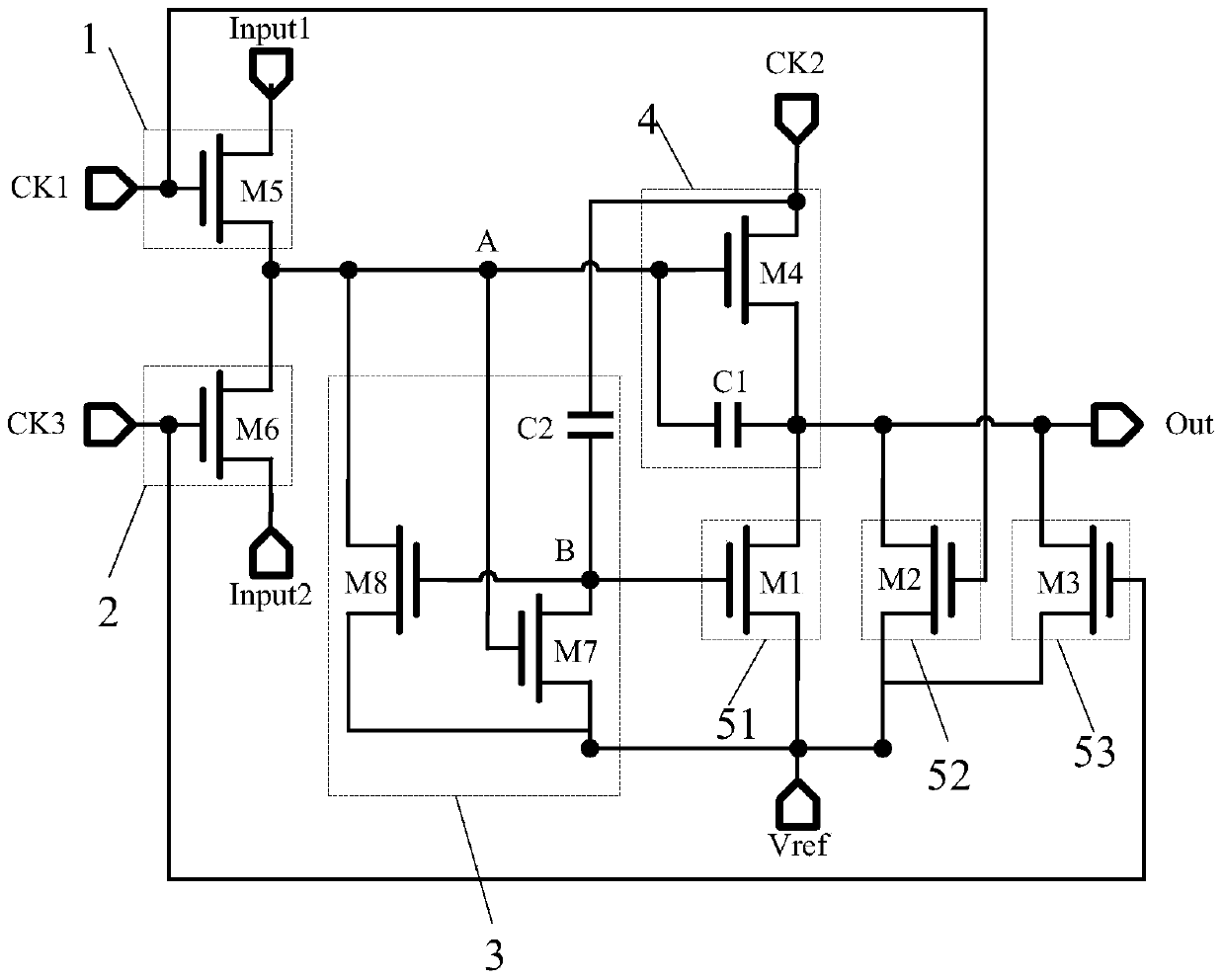
[0107] by Figure 5 The input-output timing diagram shown is an example for image 3 The working process of the shift register shown is described, specifically, select as Figure 5 The six stages of T1 ~ T6 in the input and output sequence diagram shown.

[0108] In the T1 stage, Input1=1, Input2=0, CK1=1, CK2=0, CK3=0.

[0109] Since CK1=1, the second switch transistor M2 and the fifth switch transistor M5 are turned on, and the turned-on fifth switch transistor M5 provides the high potential signal of the first input signal terminal Input1 to the first node A, so the first node A The potential of the second node B is the high potential, the fourth switch transistor M4 and the seventh switch transistor M7 are turned on, and the turned-on seventh switch transistor M7 provides the low potential signal of the reference signal terminal Vref to the second node B, and the potential of the second node B The turned-on fourth switch transistor M4 supplies the low-potential signal o...

example 2

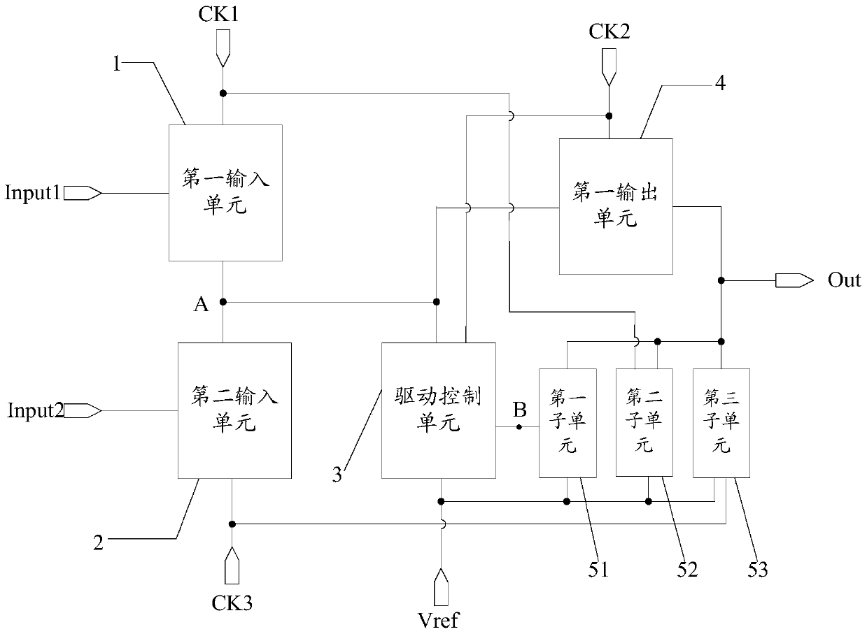
[0122] by Figure 6 The input-output timing diagram shown is an example for Figure 4 The working process of the shift register shown is described, specifically, select as Figure 6 The six stages of T1 ~ T6 in the input and output sequence diagram shown.

[0123] In the T1 stage, Input1=0, Input2=1, CK1=0, CK2=1, CK3=1.

[0124]Since CK1=1, the second switch transistor M2 and the fifth switch transistor M5 are turned on, and the turned-on fifth switch transistor M5 provides the low potential signal of the first input signal terminal Input1 to the first node A, so the first node A The potential of the second node B is low, the fourth switch transistor M4 and the seventh switch transistor M7 are turned on, and the turned-on seventh switch transistor M7 provides the high potential signal of the reference signal terminal Vref to the second node B, and the potential of the second node B The turned-on fourth switching transistor M4 supplies the high-potential signal of the secon...


PUM


Abstract

The invention discloses a shift register, its driving method and gate driving circuit. The first input unit controls the first node under the control of the first clock signal terminal and the first input signal terminal; the second input unit controls the first node at the third clock signal terminal; The first node is controlled under the control of the signal terminal and the second input signal terminal; the drive control unit controls the potentials of the first node and the second node; the first output unit controls the scan signal output terminal under the control of the first node; the second output unit The scanning signal output terminal is controlled under the control of the second node, the first clock signal terminal or the third clock signal terminal. Since the first input unit and the second input unit are designed symmetrically, the function interchange can be realized by timing matching of the signals of the input signal terminal and the clock signal terminal, so the above-mentioned shift register provided by the embodiment of the present invention can realize bidirectional scanning. Compared with the prior art, there is no need to set a separate control signal for the scanning direction, thus facilitating the design of narrow borders.

Description

technical field [0001] The invention relates to the field of display technology, in particular to a shift register, its driving method and gate driving circuit. Background technique [0002] In today's era of rapid technological development, liquid crystal displays have been widely used in electronic display products, such as televisions, computers, mobile phones and personal digital assistant devices. The liquid crystal display includes a data driver (Source Driver), a gate driver (Gate Driver), and a liquid crystal display panel. The liquid crystal display panel has a pixel array, and the gate driving device is used to sequentially turn on the corresponding pixel rows in the pixel array, so as to transmit the pixel data output by the data driver to the pixels, and then display the image to be displayed. [0003] At present, the gate driver is generally formed on the array substrate of the liquid crystal display through an array process, that is, the gate driver on array (...

Claims


Application Information

Patent Timeline
Patent Type & Authority Patents(China)
IPC IPC(8): G09G3/36
CPCG09G3/3674G09G2310/0286G11C19/28G09G3/3677G09G2310/0283G09G2310/08G11C19/184G09G3/3648G09G2310/06
Inventor 胡理科青海刚
Owner BOE TECH GRP CO LTD
Why Eureka
Try Eureka