Shift register unit, shift register and driving method, array substrate
A shift register, array substrate technology, applied in the field of array substrate, shift register and driving method, shift register unit, can solve the problems of display influence, shorten display time, poor display, etc., achieve touch control, improve display effect of effect
- Summary
- Abstract
- Description
- Claims
- Application Information
AI Technical Summary
Problems solved by technology
Method used
Image

Examples
Embodiment 1
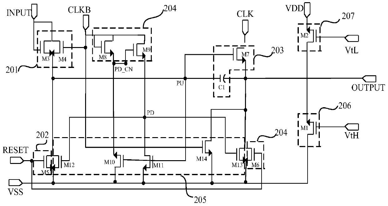
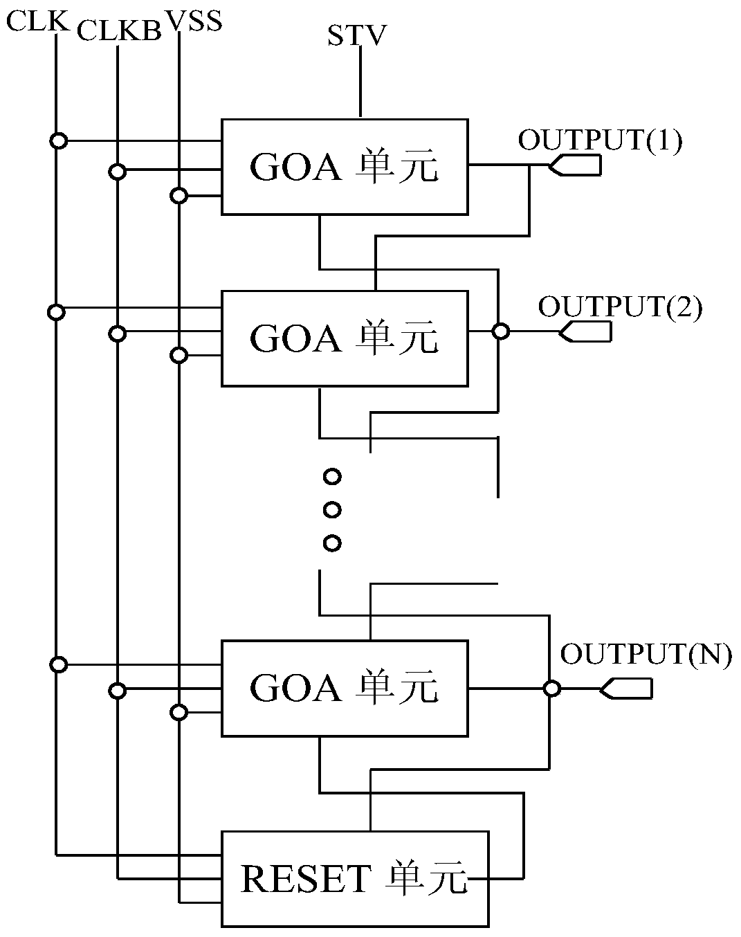
[0046] see figure 1 , a shift register unit provided by an embodiment of the present invention, the shift register unit includes an input module 201 for driving gate lines in a display panel to scan row by row, a reset module 202, a pull-up module 203, and a pull-down module 204 , an output module 205, and a touch start module 206 and a touch turn off module 207 for determining whether the display panel enters a touch stage, wherein,
[0047] The control end of the touch start module 206 is connected to the touch start signal VtH, the input end of the touch start module 206 is connected to the power supply negative signal VSS, the output end of the touch start module 206 is connected to the output terminal OUTPUT, and the touch start signal VtH is The pulse signal in the control time period; the touch start module 206, in response to the touch start signal VtH, is used to provide the negative electrode signal VSS of the power supply to the output terminal OUTPUT, so that the d...
Embodiment 2
[0088] see Figure 6 , the driving method of the shift register provided by Embodiment 1 of the present invention, the method includes:
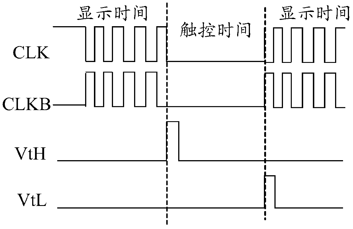
[0089] S601. When the touch time starts, the touch start module provides the negative voltage VSS of the power supply to the output terminal OUTPUT when receiving the touch start signal VtH;
[0090] S602. When the touch time is over, the touch off module provides the positive voltage VDD of the power supply to the output terminal OUTPUT when receiving the touch off signal VtL.
[0091] Wherein, the method also includes:
[0092] During the display period, when the input module receives the input signal INPUT or the second clock signal CLKB, it provides the input signal INPUT to the pull-up node PU point;
[0093] The output module provides the first clock signal CLK to the output terminal OUTPUT after receiving the voltage signal of the pull-up node PU;
[0094] When the reset module receives the reset signal RESET, it provides the negat...
PUM
 Abstract
Description
Claims
Application Information
 - R&D Engineer
- R&D Manager
- IP Professional
- Industry Leading Data Capabilities
- Powerful AI technology
- Patent DNA Extraction
Browse by: Latest US Patents, China's latest patents, Technical Efficacy Thesaurus, Application Domain, Technology Topic.
© 2024 PatSnap. All rights reserved.Legal|Privacy policy|Modern Slavery Act Transparency Statement|Sitemap