Polarization coupling device for semi-conductor laser device adopting prism

A coupling device and semiconductor technology, applied in optics, instruments, optical components, etc., can solve the problems of increasing system volume and complexity, and achieve the effect of improving beam quality and optical power density, high brightness and high power laser output

Inactive Publication Date: 2013-07-24
INST OF SEMICONDUCTORS - CHINESE ACAD OF SCI
View PDF5 Cites 13 Cited by
  • Summary
  • Abstract
  • Description
  • Claims
  • Application Information

AI Technical Summary

Problems solved by technology

Adding too many components in the optical path wil...

Method used


Image

  • Polarization coupling device for semi-conductor laser device adopting prism
  • Polarization coupling device for semi-conductor laser device adopting prism
  • Polarization coupling device for semi-conductor laser device adopting prism

Examples


no. 1 example

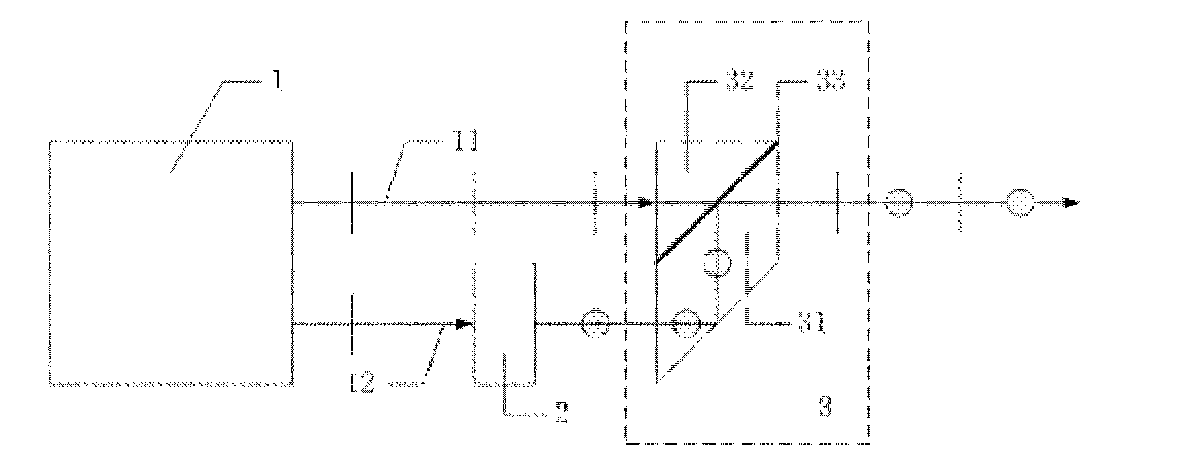
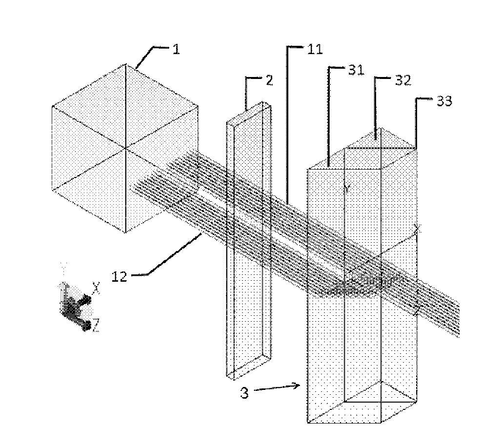
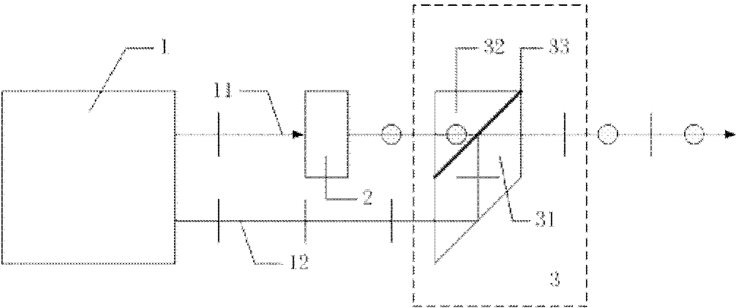
[0019] see figure 1 and figure 2 Shown, be the first embodiment of the present invention, the present invention provides a kind of semiconductor laser polarization coupling device that adopts prism, comprising:

[0020] A semiconductor laser array 1 . The semiconductor laser array includes fast-axis collimation elements, and may also include slow-axis collimation elements. The beam emitted by the semiconductor laser array has a very small divergence angle in the y direction after being collimated by the fast axis, which can basically be ignored. The light beam emitted by the semiconductor laser array can also be collimated by the slow axis to reduce the divergence angle in the x direction to a certain extent. After collimation, the beam emitted by the semiconductor laser array has a total width of 10 mm in the x direction and can be divided into two paths, each of which has a width of 5 mm in the x direction. Wherein, the one that deviates to the positive direction of the...


PUM


Abstract

The invention discloses a polarization coupling device for a semi-conductor laser device adopting a prism. The device comprises a semi-conductor laser device array, a halfwave plate and a polarization beam split prism, wherein the semi-conductor laser device array comprises a first output light path and a second output light path; the halfwave plate is arranged on the second output light path of the semi-conductor laser device array; and the polarization beam split prism is arranged on the second output light path and the first output light path of the semi-conductor laser device array, and the halfwave plate is arranged between the semi-conductor laser device array and the polarization beam split prism. According to the device, the size of output light beam of the semi-conductor laser device array can be compressed, and the brightness and the quality of the light beam can be improved.

Description

technical field [0001] The invention belongs to the field of laser optoelectronics and its application, and is a polarization coupling device for a semiconductor laser using a prism, which performs polarization coupling on the output beam of a semiconductor laser through a parallelogram prism, a triangular prism and a polarization splitting film, and improves the brightness and beam quality of the output beam. . Background technique [0002] Semiconductor lasers have the advantages of high photoelectric conversion efficiency, small size, and long life, and are widely used in various applications such as pumping solid-state lasers, medical treatment, and material processing. Semiconductor laser arrays (including one-dimensional semiconductor laser arrays and two-dimensional semiconductor laser stacked arrays—stacks) are an effective way to achieve high power output. However, the beam quality of semiconductor laser arrays limits the application range of semiconductor lasers. ...

Claims


Application Information

Patent Timeline
IPC IPC(8): G02B27/28
Inventor 林学春郭渭荣陈凯王宝华王祥鹏王丽荣
Owner INST OF SEMICONDUCTORS - CHINESE ACAD OF SCI
Why Eureka
Try Eureka