Multilayer chip inductor and manufacturing method thereof

A manufacturing method and inductor technology, which is applied in the manufacture of inductors/transformers/magnets, inductors, fixed inductors, etc., can solve problems such as low rated current and limited scope of application, and achieve the effect of increasing the rated current

Active Publication Date: 2014-03-26
SHENZHEN ZHENHUA FU ELECTRONICS
View PDF8 Cites 9 Cited by
  • Summary
  • Abstract
  • Description
  • Claims
  • Application Information

AI Technical Summary

Problems solved by technology

[0003] However, the traditional multilayer chip inductors have a low rated current, which limits their application range

Method used


Image

  • Multilayer chip inductor and manufacturing method thereof
  • Multilayer chip inductor and manufacturing method thereof

Examples


Embodiment Construction

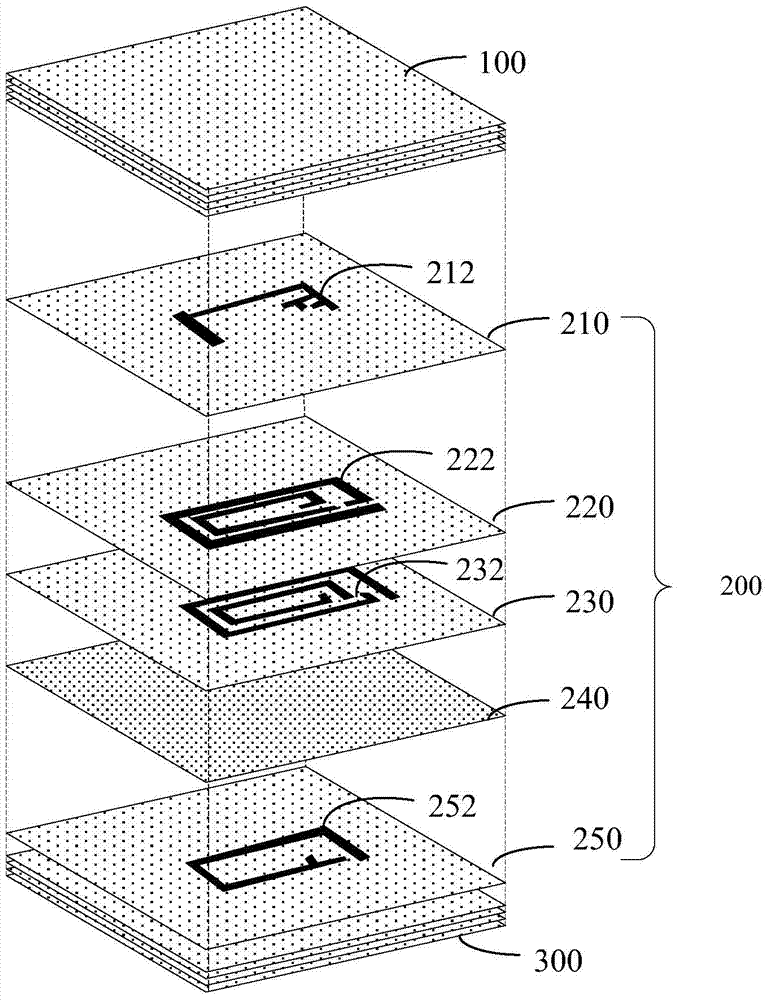
[0025] Such as figure 1 Shown is a structural diagram of a multilayer chip inductor of an embodiment. The multilayer chip inductor includes a first cover 100 , an intermediate layer 200 and a second cover 300 stacked in sequence.

[0026] Wherein the first cover 100 and the second cover 300 are ferrite material diaphragms without perforation. The intermediate layer 200 includes a first wiring layer 210 , a first dielectric layer 220 , a second dielectric layer 230 , a non-magnetic isolation layer 240 and a second wiring layer 250 stacked in sequence. Both the first cover 100 and the second cover 300 are composed of more than one layer of ferrite material membranes, that is, the thickness of the first cover 100 and the second cover 300 is greater than or equal to that of each layer printed with electrode coils. The thickness of the dielectric layer.

[0027] The first lead layer 210 is close to the first cover 100 , and the second lead layer 250 is close to the second cover ...


PUM


Abstract

Provided is a multilayer chip inductor. The multilayer chip inductor comprises a first cover body, a middle layer and a second cover body, wherein the first cover body, the middle layer and the second cover body are stacked in sequence, the middle layer comprises a lead layer which is stacked in a parallel mode, and more than two dielectric layers, electrode coils are printed on the dielectric layers, wires of the electrode coils on every two adjacent dielectric layers are distributed in a parallel and parallel connection mode, and the lead layer is close to the first cover body or the second cover body. The rated current of the multilayer chip inductor can be greatly increased, and the multilayer chip inductor can be widely applied to electronic devices such as computers and communication machines.

Description

technical field [0001] The invention relates to the field of electronic components, in particular to a laminated chip inductor and a manufacturing method thereof. Background technique [0002] With the development of industrial automation, especially the development of modern communication industry (such as mobile phones and other portable terminal products), multilayer chip inductors have become the key products in the field of inductive components due to their advantages of good magnetic shielding and miniaturization. Its applications range from mobile devices, computers, servers, personal navigation systems, personal multimedia devices, and automotive systems. [0003] However, the traditional multilayer chip inductors have a low rated current, which limits their scope of application. Contents of the invention [0004] Based on this, it is necessary to provide a multilayer chip inductor with high rated current and a manufacturing method thereof. [0005] A laminated c...

Claims


Application Information

Patent Timeline
Patent Type & Authority Applications(China)
IPC IPC(8): H01F37/00H01F27/29H01F27/28H01F1/113H01F41/00
Inventor 王振兴徐鹏飞李建辉刘季超樊应县李耀坤庞岩王智会
Owner SHENZHEN ZHENHUA FU ELECTRONICS
Why Eureka
Try Eureka