
pop placement device and its chip removal jig

A patch device and chip technology, applied in the direction of electrical components, electrical components, etc., can solve problems such as poor welding

Inactive Publication Date: 2017-02-01
GUANGDONG OPPO MOBILE TELECOMM CORP LTD
View PDF11 Cites 0 Cited by
  • Summary
  • Abstract
  • Description
  • Claims
  • Application Information

AI Technical Summary

Problems solved by technology

[0004] Based on this, the present invention overcomes the defects of the prior art and provides a POP placement device, which can effectively avoid the problem of poor soldering caused by chip falling off during the placement process.

Method used


Image

  • pop placement device and its chip removal jig
  • pop placement device and its chip removal jig

Examples


Embodiment Construction

[0025] The embodiments of the present invention will be described in detail below in conjunction with the drawings:

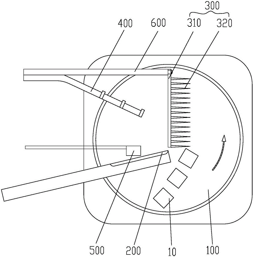
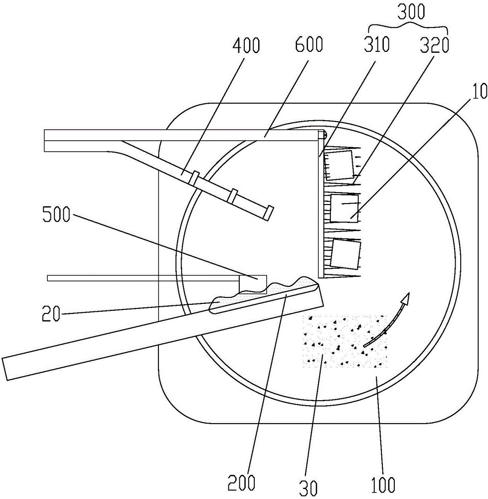
[0026] Reference figure 1 , figure 2 , A POP placement device, including a turntable 100, a scraper 200 and a chip removal jig 300 disposed above the turntable 100, the chip removal jig 300 includes a horizontal frame 310, a plurality of stop bars 320, the stop bars 320 is installed on the horizontal frame 310 at intervals, and the end of the barrier 320 away from the horizontal frame 310 is in contact with the surface of the turntable 100 or slightly higher than the surface of the turntable 100, and it is opposite to the direction in which the turntable 100 rotates.

[0027] In the POP placement device of this embodiment, by setting the chip removal jig 300 on the turntable 100, once the chip 10 falls off into the turntable 100 when the solder is dipped in the flux area 30, the chip 10 will follow The turntable 100 rotates to the chip removal jig 300, the stop ba...


PUM


Abstract

The invention discloses a POP paster device which comprises a turntable, a scraper arranged above the turntable and a chip removing jig. The chip removing jig comprises a transverse frame and multiple blocking strips, wherein the blocking strips are installed on the transverse frame at intervals, one end of each blocking strip away from the transverse frame is in contact with the turntable surface and opposite to the turntable in rotation direction. The chip removing jig is arranged on the turntable, once a chip drops into the turntable, the chip rotates to the position of the chip removing jig with the turntable, the blocking strips block the chip, the chip can slip onto the blocking strips under the driving of the turntable and break away from the turntable and is prevented from rotating to the scraper position and influencing normal flowing of a bottom layer scaling powder, follow-up chips can dip in the scaling powder, and the poor welding problem caused by the fact that upper-layer chips drop is solved. In addition, the blocking strips are arranged on the transverse frame at intervals, the scaling powder can pass through the separation positions, and normal flowing of the scaling powder is not influenced. The invention further discloses the chip removing jig.

Description

Technical field [0001] The invention relates to a POP patch device and a chip removal jig. Background technique [0002] At present, the specific process of POP (Package on Package) packaged device mounting process is as follows: First, put the flux in the turntable set on the SMT (Surface Mounted Technology) mounter rack, and use the scraper to smooth the flux. The SMT placement machine sucks the upper chip and moves it to the top of the turntable, so that all the solder balls under the upper chip are dipped in flux, and then the upper chip is placed on the bottom chip to bond the upper chip and the bottom chip to each other, and finally The bonded chips are sent to a reflow oven for soldering. As the tin balls melt, high-quality tin alloy soldering is formed between the upper chip and the bottom chip of the POP package device. [0003] In the above process, the upper layer chip often comes off when dipped in the flux. After the upper layer chip falls off the turntable, it rotate...

Claims


Application Information

Patent Timeline
Patent Type & Authority Patents(China)
IPC IPC(8): H05K13/04
Inventor 王之新
Owner GUANGDONG OPPO MOBILE TELECOMM CORP LTD
Learn More