Eureka AIR delivers breakthrough ideas for toughest innovation challenges, trusted by R&D personnel around the world.

Liquid crystal panel and manufacturing method thereof and liquid crystal display device

A liquid crystal panel and liquid crystal layer technology, applied in nonlinear optics, instruments, optics, etc., can solve problems such as unilateral or multilateral chromatic aberration, smaller gaps, and uneven overall size of the plastic frame in the display area, so as to reduce peripheral chromatic aberration , Improve the effect of display quality

Active Publication Date: 2015-04-29
TCL CHINA STAR OPTOELECTRONICS TECH CO LTD
View PDF6 Cites 5 Cited by
  • Summary
  • Abstract
  • Description
  • Claims
  • Application Information

AI Technical Summary

Problems solved by technology

In the manufacturing process, one situation is that the upper and lower sides of the plastic frame will be provided with metal wires, and the unevenness of the wires will make the overall size of the plastic frame uneven, which will easily lead to a gap between the array substrate and the color filter substrate in the transition area. Smaller, that is, the glass layer of the array substrate or color filter substrate facing the liquid crystal layer is deformed, resulting in unilateral or multilateral chromatic aberration around the display area, which seriously affects the display quality of the display area

Method used


Image

  • Liquid crystal panel and manufacturing method thereof and liquid crystal display device
  • Liquid crystal panel and manufacturing method thereof and liquid crystal display device
  • Liquid crystal panel and manufacturing method thereof and liquid crystal display device

Examples


Embodiment Construction

[0023] The following will clearly and completely describe the technical solutions in the embodiments of the present invention with reference to the accompanying drawings in the embodiments of the present invention. Obviously, the described embodiments are only some, not all, embodiments of the present invention. Based on the embodiments of the present invention, all other embodiments obtained by persons of ordinary skill in the art without creative efforts fall within the protection scope of the present invention.

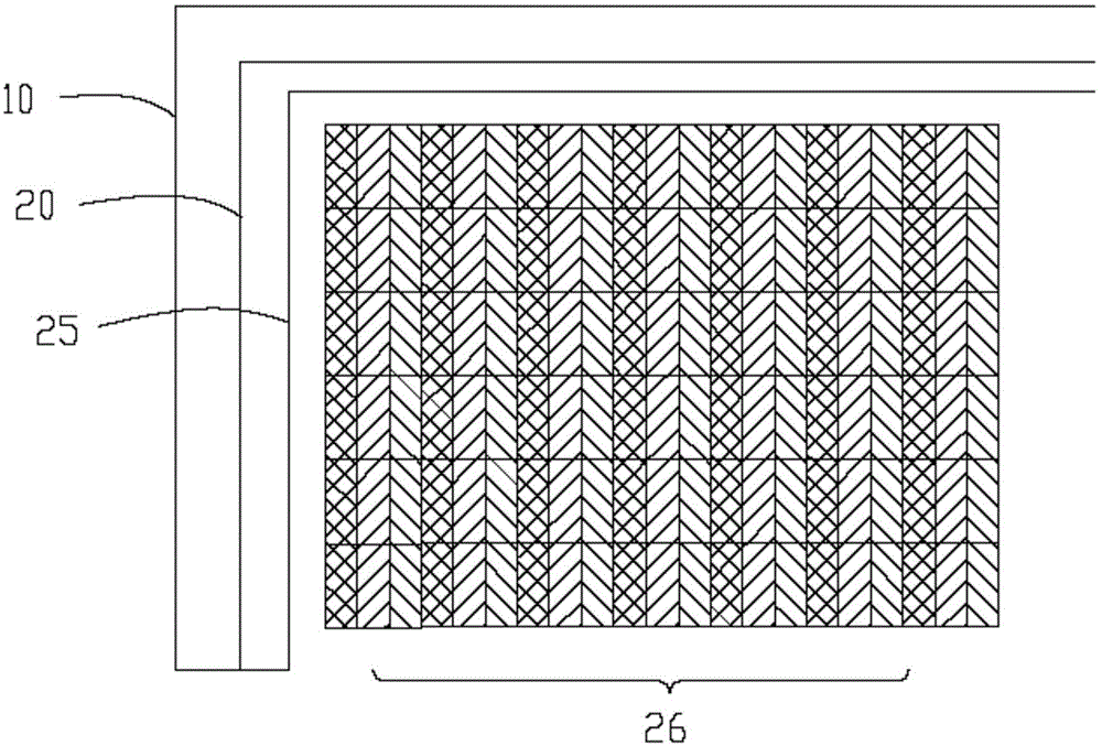
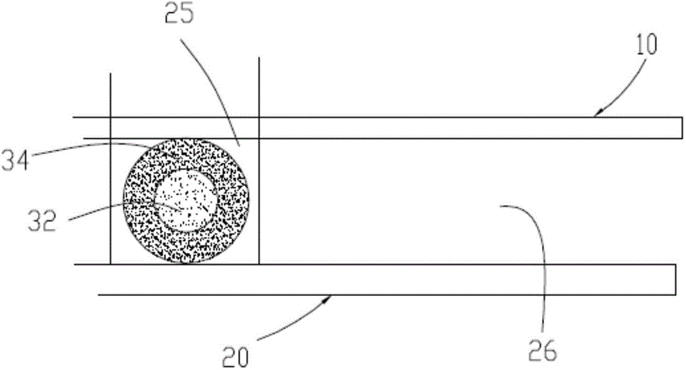
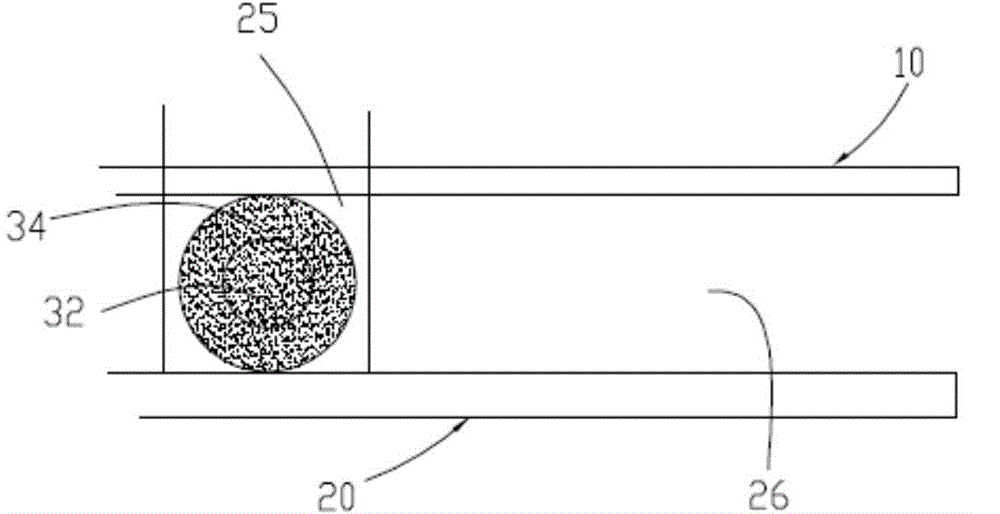
[0024] see figure 1 and figure 2 , a liquid crystal panel, comprising a first substrate 10 and a second substrate 20 opposite to the first substrate 10, a liquid crystal layer sandwiched between the first substrate 10 and the second substrate 20 and a liquid crystal layer located in the first The sealant frame 25 between the substrate 10 and the second substrate 20 seals the liquid crystal layer, and the position of the liquid crystal layer surrounded by the seal...


PUM

PropertyMeasurementUnit
heightaaaaaaaaaa
widthaaaaaaaaaa
diameteraaaaaaaaaa

Abstract

The invention provides a liquid crystal panel. The liquid crystal panel comprises a first substrate, a second substrate, a liquid crystal layer and a sealant box, wherein the second substrate is arranged opposite to the first substrate; the liquid crystal layer is clamped between the first substrate and the second substrate; the sealant box is positioned on the liquid crystal layer between the first substrate and the second substrate; the liquid crystal layer surrounded by the sealant box is positioned in a display region of the liquid crystal panel; a spherical supporting object is arranged in the sealant box and comprise an inner layer and an outer layer; at least one layer of the outer layer and the inner layer is made of a thermal expansion material; or the inner layer and the outer layer are both made of the thermal expansion material. The invention provides a manufacturing method of the liquid crystal panel and a liquid crystal display device.

Description

technical field [0001] The invention relates to the technical field of liquid crystal display, in particular to a liquid crystal panel, a manufacturing method and a liquid crystal display device. Background technique [0002] At present, liquid crystal display devices have been widely used in various electronic products as display components of electronic equipment. A liquid crystal is formed between the color filter substrate and the array substrate to form a plastic frame for sealing the liquid crystal. A support is provided between the color filter substrate and the array substrate, so that a display area is formed on the liquid crystal panel, and the display area is arranged around the display area. Transition area, the glue frame set around the transition area. In the manufacturing process, one situation is that the upper and lower sides of the plastic frame will be provided with metal wires, and the unevenness of the wires will make the overall size of the plastic fra...

Claims


Application Information

Patent Timeline
Patent Type & Authority Applications(China)
IPC IPC(8): G02F1/1339
CPCG02F1/13392G02F1/13398G02F1/1339G02F1/133514G02F1/1341
Inventor 唐岳军
Owner TCL CHINA STAR OPTOELECTRONICS TECH CO LTD
Why Eureka
Eureka Blog
Learn More