
Liquid crystal panel and manufacturing method thereof and liquid crystal displaying device

a technology of liquid crystal panels and displaying devices, which is applied in non-linear optics, instruments, optics, etc., can solve the problems of excessively large or excessively small compression, deformation of the substrate supported by the resin frame, and non-uniformity of the entire size, so as to improve the displaying quality the perimeter color difference of the liquid crystal panel

Active Publication Date: 2017-06-06
TCL CHINA STAR OPTOELECTRONICS TECH CO LTD
View PDF2 Cites 0 Cited by
  • Summary
  • Abstract
  • Description
  • Claims
  • Application Information

AI Technical Summary

Benefits of technology

The present invention is about improving the quality of liquid crystal displays by reducing color differences at the edges of the display. This is done by using a special resin frame and supports made of a substance that can change its size when exposed to light and heat. By adjusting the gap between the two substrates, the supports help to minimize the differences in color between the edges of the display, resulting in a better quality image.

Problems solved by technology

During the manufacture, one situation is that metal wiring is arranged under the resin frame and non-uniformity of the wiring may cause non-uniformity of the entire size of the resin frame, leading to deformation of the substrates supported by the resin frame.
Another situation is that the density of the supports in the transition zone is small so as to cause excessively large or excessively small compression.
In other words, the glass layer of the array substrate or the color filter substrate that faces the liquid crystal layer may gets deformed, leading to color difference occurring at one side or multiple sides around the displaying zone so as to severely affect the displaying quality of the displaying zone.

Method used


Image

  • Liquid crystal panel and manufacturing method thereof and liquid crystal displaying device
  • Liquid crystal panel and manufacturing method thereof and liquid crystal displaying device
  • Liquid crystal panel and manufacturing method thereof and liquid crystal displaying device

Examples


Embodiment Construction

[0032]A clear and complete description will be given to technical solutions of the embodiments of the present invention with reference to the attached drawings of the embodiments of the present invention. However, the embodiments so described are only some, but not all, of the embodiments of the present invention. Other embodiments that are available to those having ordinary skills of the art without the expense of creative effort and endeavor are considered belonging to the scope of protection of the present invention.

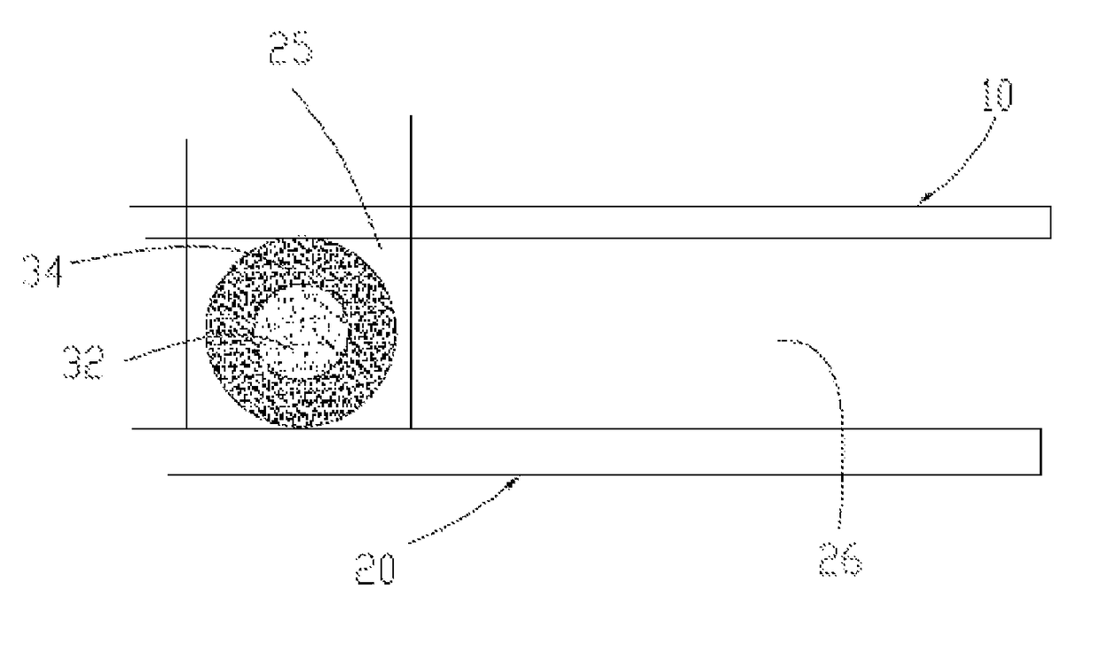
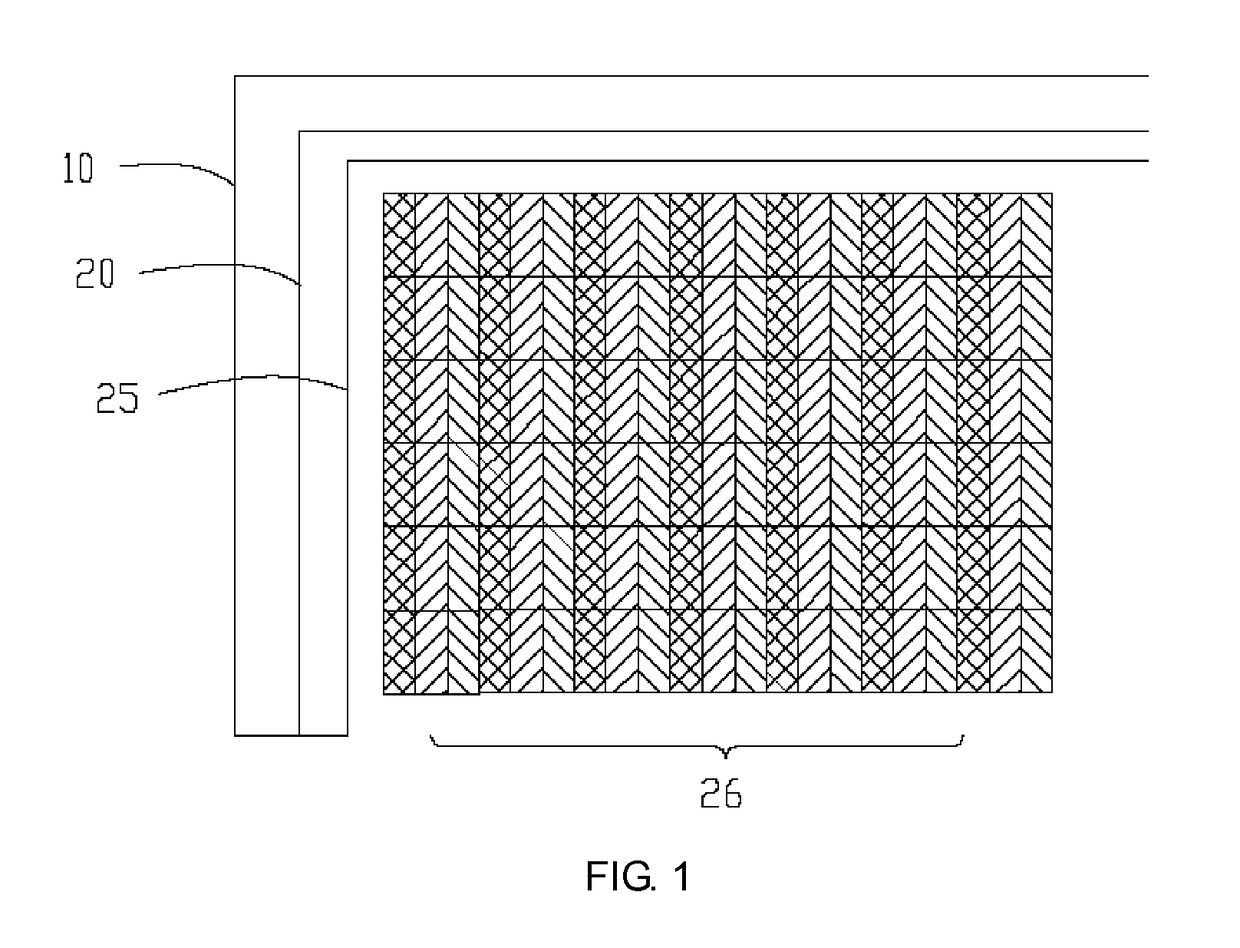
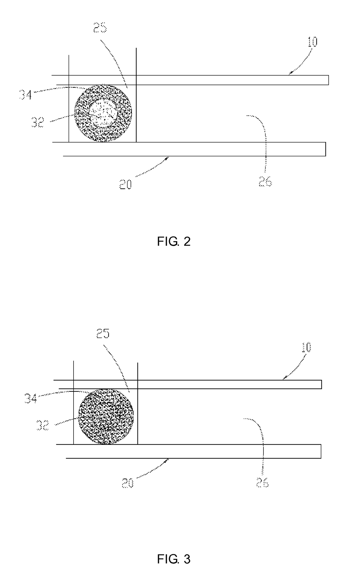
[0033]Referring to FIGS. 1 and 2, a liquid crystal panel comprises a first substrate 10 and a second substrate 20 opposite to the first substrate 10, a liquid crystal layer interposed between the first substrate 10 and the second substrate 20, and an enclosure resin frame 25 located between the first substrate 10 and the second substrate 20 to enclose and seal the liquid crystal layer. The enclosure resin frame 25 surrounds the liquid crystal layer that is located in ...


PUM

PropertyMeasurementUnit
widthaaaaaaaaaa
heightaaaaaaaaaa
diameteraaaaaaaaaa

Abstract

A liquid crystal panel includes a first substrate and a second substrate opposite to the first substrate, a liquid crystal layer interposed between the first substrate and the second substrate, and an enclosure resin frame located between the first substrate and the second substrate to enclose and seal the liquid crystal layer. The enclosure resin frame surrounds the liquid crystal layer that is located in a displaying zone of the liquid crystal panel. The enclosure resin frame includes spherical supports arranged therein. The spherical supports include an inner layer and an outer layer. At least one of the outer layer and the inner layer is made of a heat-shrinkable material, or alternatively, the inner layer and the outer layer are both made of heat-shrinkable materials. Also provided are a manufacturing method of a liquid crystal panel and a liquid crystal displaying device.

Description

CROSS REFERENCE TO RELATED APPLICATIONS[0001]This application claims the priority of Chinese Patent Application No. 201410844703.2, entitled “Liquid Crystal Panel and Manufacturing Method Thereof and Liquid Crystal Displaying Device”, filed on Dec. 30, 2014, the disclosure of which is incorporated herein by reference in its entirety.BACKGROUND OF THE INVENTION[0002]1. Field of the Invention[0003]The present invention relates to the field of liquid crystal displaying, and in particular to a liquid crystal panel, a manufacturing method, and a liquid crystal displaying device.[0004]2. The Related Arts[0005]Currently, liquid crystal display devices, serving as display components of electronic devices, have been widely used in various electronic products for liquid crystal displaying. A liquid crystal panel comprises an array substrate and a color filter substrate that are opposite to each other and liquid crystal interposed between the array substrate and the color filter substrate. A r...

Claims


Application Information

Patent Timeline
Patent Type & Authority Patents(United States)
IPC IPC(8): G02F1/1339G02F1/1341
CPCG02F1/1339G02F1/1341G02F1/13394G02F2001/13398G02F1/13398
Inventor TANG, YUEJUN
Owner TCL CHINA STAR OPTOELECTRONICS TECH CO LTD
Learn More