Layout design method, layout design system and manufacture method of integrated circuit

A technology of integrated circuit and layout design, applied in computing, electrical digital data processing, instruments, etc., can solve the problems of low yield rate of integrated circuits, well proximity effect and shallow trench isolation stress effect, etc., to improve and lengthen the design cycle Effect

Active Publication Date: 2015-09-16
INST OF MICROELECTRONICS CHINESE ACAD OF SCI
View PDF2 Cites 21 Cited by
  • Summary
  • Abstract
  • Description
  • Claims
  • Application Information

AI Technical Summary

Problems solved by technology

Due to the further shrinking of the size of the transistor, the characteristics of the transistor itself are more significantly affected by the layout dependent effect, such as the influence of the well proximity effect and the shallow trench isolation stress effect, which in turn leads to the production yield of the integrated circuit. Low

Method used


Image

  • Layout design method, layout design system and manufacture method of integrated circuit
  • Layout design method, layout design system and manufacture method of integrated circuit
  • Layout design method, layout design system and manufacture method of integrated circuit

Examples


Embodiment Construction

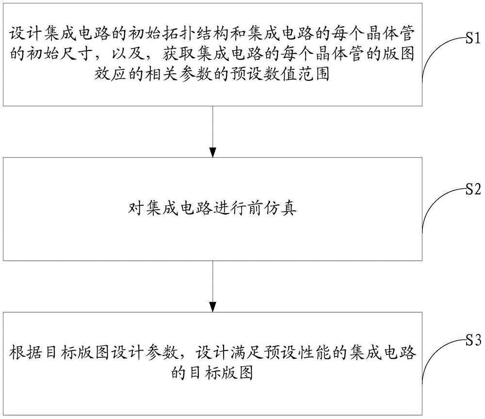
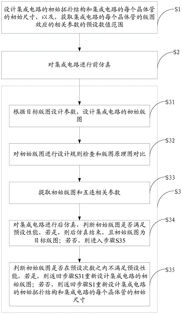
[0038] The following will clearly and completely describe the technical solutions in the embodiments of the present invention with reference to the accompanying drawings in the embodiments of the present invention. Obviously, the described embodiments are only some, not all, embodiments of the present invention. Based on the embodiments of the present invention, all other embodiments obtained by persons of ordinary skill in the art without making creative efforts belong to the protection scope of the present invention.

[0039] As mentioned in the background technology, due to the further shrinkage of the transistor size, the characteristics of the transistor itself are more significantly affected by the layout dependent effect, such as the effect of the well proximity effect and the shallow trench isolation stress effect, which in turn leads to integration The production yield of the circuit is low.

[0040] Based on this, the embodiment of the present application provides a ...


PUM


Abstract

The invention discloses a layout design method, a layout design system and a manufacture method of an integrated circuit. The design method comprises the steps as follows: designing an initial topological structure of the integrated circuit and an initial size of each transistor of the integrated circuit, and obtaining a preset numerical range of a relevant parameter of a layout effect of each transistor of the integrated circuit; performing pre-simulation to the initial topological structure of the integrated circuit, the initial size of each transistor and relevant parameter of the layout effect of each transistor so as to obtain a target layout design parameter which meets a preset yield rate, wherein the target layout design parameter comprises a target topological structure of the integrated circuit, a target size of each transistor of the integrated circuit, and a target numerical value of the relevant parameter of the layout effect of each transistor of the integrated circuit; designing a target layout of the integrated circuit meeting preset performance according to the target layout design parameter. The layout design method, the layout design system and the manufacture method of the invention ensure the yield rate for manufacturing the integrated circuit and improve the condition that the design cycle is long while designing current layout.

Description

technical field [0001] The present invention relates to the technical field of integrated circuits, and more specifically, relates to a layout design method, a layout design system and a manufacturing method of an integrated circuit. Background technique [0002] Today, with the continuous advancement of integrated circuit technology to the node process, the feature size of transistors has also increased from the previous micron level to the nanometer level. Due to the further shrinking of the size of the transistor, the characteristics of the transistor itself are more significantly affected by the layout dependent effect, such as the influence of the well proximity effect and the shallow trench isolation stress effect, which in turn leads to the production yield of the integrated circuit. Low. Contents of the invention [0003] In view of this, the present invention provides a layout design method, a layout design system and a manufacturing method of an integrated circu...

Claims


Application Information

Patent Timeline
Patent Type & Authority Applications(China)
IPC IPC(8): G06F17/50
Inventor 孙建伟陈岚王海永
Owner INST OF MICROELECTRONICS CHINESE ACAD OF SCI
Why Eureka
Try Eureka