

Electronic component
A technology of electronic components and circuit components, applied to electrical components, parts of transformers/inductors, circuits, etc., can solve problems such as fracture and grain boundary cracks
- Summary
- Abstract
- Description
- Claims
- Application Information
AI Technical Summary
Problems solved by technology
Method used
Image

Examples
Example
[0022] (First embodiment)
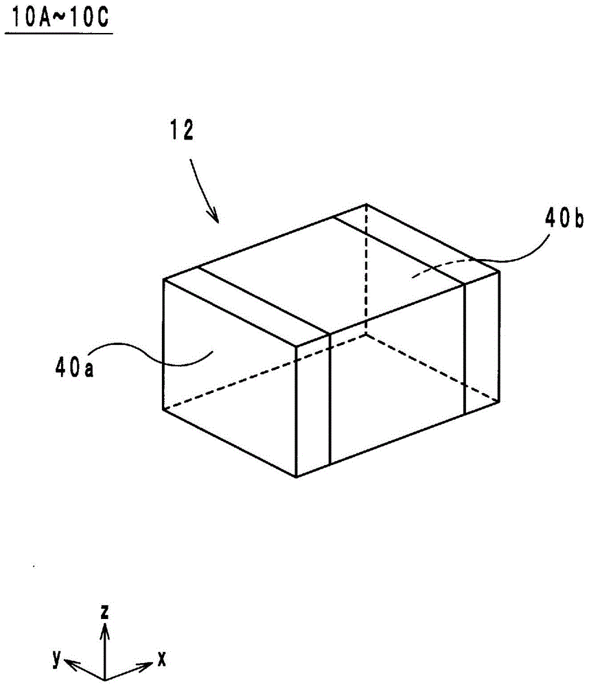
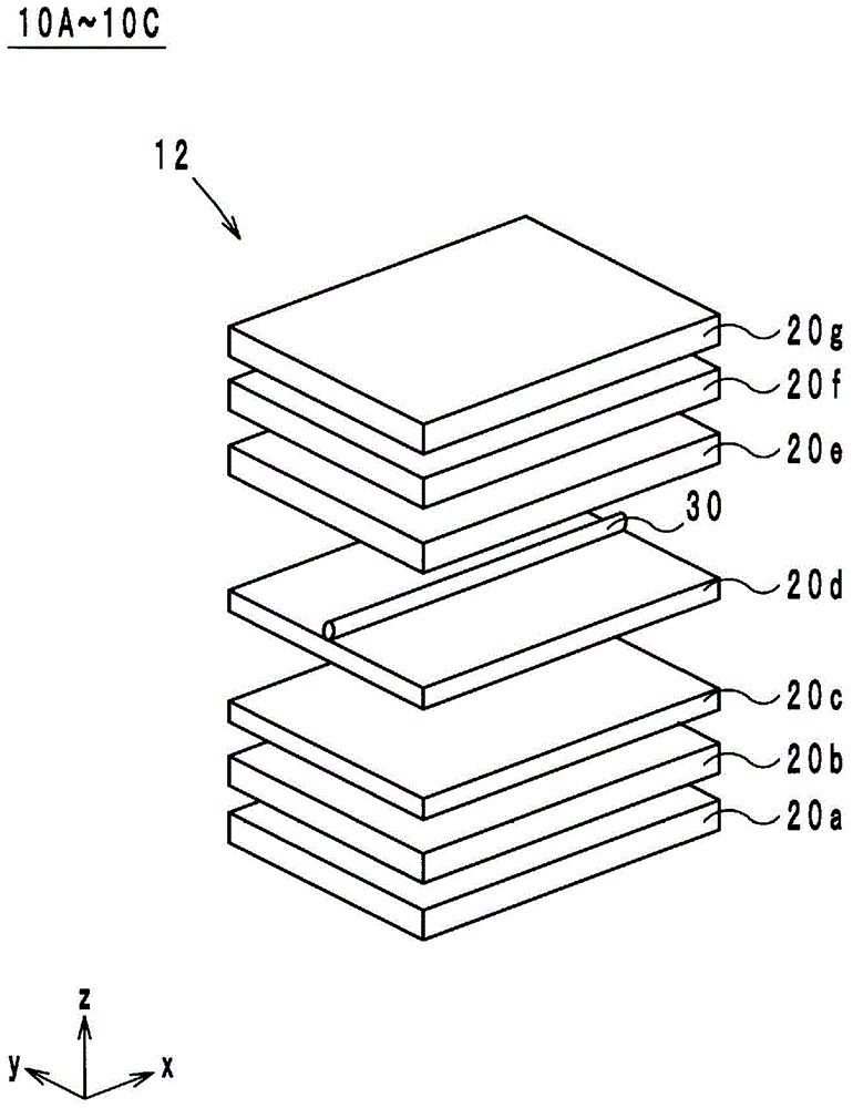
[0023] Hereinafter, the electronic component 10A as the first embodiment will be described with reference to the drawings. figure 1 It is an external perspective view of the electronic component 10A as the first embodiment. figure 2 It is an exploded perspective view of the laminated body 12 in the electronic component 10A as the first embodiment. Hereinafter, the stacking direction of the electronic component 10A is defined as the z-axis direction, and the direction along the long side of the electronic component 10A when viewed from the z-axis direction is defined as the x-axis direction. In addition, the direction along the short side of the electronic component 10A when viewed from the z-axis direction is defined as the y-axis direction. It should be noted that the x-axis, y-axis, and z-axis are orthogonal to each other.
[0024] Electronic components 10A such as figure 1 Shown is a rectangular parallelepiped. In addition, the electronic compone...
Example
[0046] (Second embodiment)
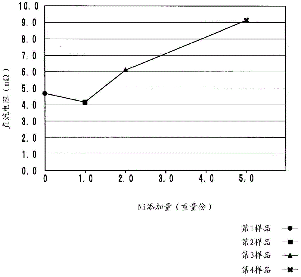
[0047] In the electronic component 10B as the second embodiment, the material of the internal conductor 30 is copper, and the surface of the internal conductor 30 is plated with nickel. The other structure is the same as the above-mentioned first embodiment. Therefore, the description of the second embodiment other than the internal conductor 30 is as described in the above-mentioned first embodiment.
[0048] With the electronic component 10B as the second embodiment, it is possible to suppress the DC resistance value after firing from being greater than the DC resistance value before firing. Specifically, in the electronic component 10B, nickel covers the surface of the internal conductor 30. This suppresses the occurrence of cracks in the internal conductor 30 of the electronic component 10B during firing. As a result, the DC resistance value after firing can be suppressed from being greater than the DC resistance value before firing.
[0049] In a...
Example
[0050] (3rd embodiment)
[0051] In the electronic component 10C as the third embodiment, the material of the internal conductor 30 is copper, and the surface of the internal conductor 30 is plated with iron. The other structure is the same as the above-mentioned first embodiment. Therefore, descriptions other than the internal conductor 30 in the third embodiment are as described in the above-mentioned first embodiment.
[0052] With the electronic component 10C as the third embodiment, it is possible to suppress the DC resistance value after firing from being greater than the DC resistance value before firing. Specifically, in the electronic component 10C, iron covers the surface of the internal conductor 30. This suppresses the occurrence of cracks in the internal conductor 30 during the firing of the electronic component 10C. As a result, the DC resistance value after firing can be suppressed from being greater than the DC resistance value before firing.
[0053] In addition,...
PUM
 Abstract
Description
Claims
Application Information