
An error-proof consumable chip and control method

A consumable chip and control method technology, which is applied to printing, printing devices, etc., can solve the problems of the printer cannot be used normally, the memory of the consumable chip works abnormally, and the number of times is small, so as to ensure the integrity and stability of data and high security. , The effect of data access and read and write convenience

Active Publication Date: 2017-10-03
HANGZHOU CHIPJET TECH CO LTD
View PDF5 Cites 0 Cited by
  • Summary
  • Abstract
  • Description
  • Claims
  • Application Information

AI Technical Summary

Problems solved by technology

However, the test at this stage is a general test with a limited range and a small number of tests. As a result, in actual use, if the working environment changes, such as voltage instability, power failure, etc., the memory of the consumable chip will work abnormally. , the data originally to be stored in the chip is wrong, which leads to the failure of the entire printer

Method used


Image

  • An error-proof consumable chip and control method
  • An error-proof consumable chip and control method
  • An error-proof consumable chip and control method

Examples


Embodiment 1

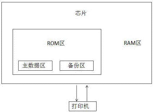
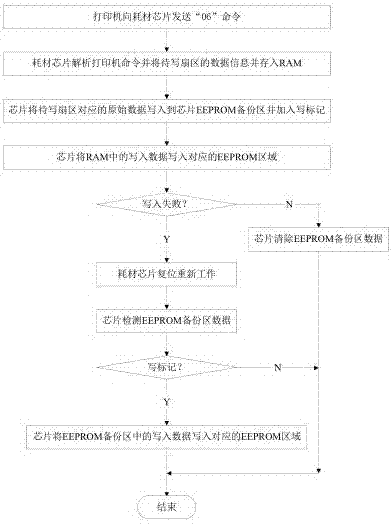
[0057] Example 1, such as figure 1 and figure 2 Shown: an error-proof consumable chip, including a chip control circuit, a data storage unit for storing data, a communication unit for communicating with a printer,

[0058]The data storage unit includes a ROM area and a RAM area. The ROM area includes the main data area and the backup area; the RAM area is used to temporarily store the written data sent by the printer to the chip of the anti-error consumable; the main data area stores the initial data; the backup area Used to save the initial data; the main data area can receive the written data from the RAM area, and overwrite the written data to replace the initial data. In this embodiment, the ROM area is EEPROM.

[0059] The original initial data of this kind of anti-error consumable chip is stored in the main data area. When the printer sends a write command, it needs to write new data, that is, the written data is written. The written data does not directly overwrite a...

Embodiment 2

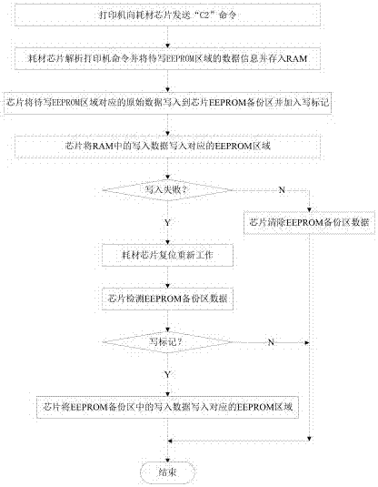
[0089] Embodiment 2: The difference from Embodiment 1 is step 1 and step 2. In step 1, the information written into the data contains a check code, while in step 2, the command sent is device address + fixed word Section + feedback data, the device address is 1 byte, and its value can be 0x60, 0x62, 0x64, 0x66 and 0x68; the value of the fixed byte is 0x82; the feedback data is a check code, which is used by the printer to judge whether it is an original consumable, Its length is the number of bytes of the feedback data in the command 1 sent by the consumable chip.


PUM


Abstract

The invention belongs to the field of ink-jet printing and particularly relates to an anti-error consumable chip and a control method thereof. According to the technical scheme, the anti-error consumable chip comprises a chip control circuit and a data storage unit for storing data. The data storage unit comprises an ROM region and an RAM region. The ROM region comprises a main data region and a backup region. The RAM region is used for temporarily storing write-in data transmitted to the anti-error consumable chip by a printer. Initial data is preserved in the main data region. The backup region is used for preserving the initial data. The main data region can receive the write-in data from the RAM region and covering and replacing the initial data with the write-in data. According to the anti-error consumable chip and the control method thereof, even though under certain abnormal conditions, the data storage unit of the consumable chip goes wrong, a system can restore normal data, and normal use of consumables is not affected.

Description

technical field [0001] The invention belongs to the field of inkjet printing, and in particular relates to an anti-error consumable chip and a control method. Background technique [0002] With the popularization of office automation, printing equipment has become an indispensable equipment in office activities. During the printing process, printer hosts and consumables such as ink cartridges are needed. In the use stage of the consumables, the parameter data and usage data of the consumables themselves are needed. These data are stored in the consumable chips, and the accuracy, stability, and integrity of these data have a great impact on the correct use of the consumables, which has a great impact on the consumables. Chips have higher requirements for data processing. [0003] In order to ensure the stability of the data processed by the consumable chip, the manufacturers of each chip will test it when the chip process is taped out. However, the test at this stage is a g...

Claims


Application Information

Patent Timeline
Patent Type & Authority Patents(China)
IPC IPC(8): B41J2/175B41J29/393
CPCB41J2/17543B41J29/393
Inventor 章征东孙云
Owner HANGZHOU CHIPJET TECH CO LTD
Learn More