Five-pin IC structure
A technology of pins and left pins, applied in the direction of electrical components, electric solid devices, circuits, etc., can solve the problems of waste of pin materials, vacant pins, complex processing technology, etc., to improve heat dissipation efficiency, reduce overall width, The effect of reducing wasted pins
- Summary
- Abstract
- Description
- Claims
- Application Information
AI Technical Summary
Problems solved by technology
Method used
Image


Examples
Embodiment Construction
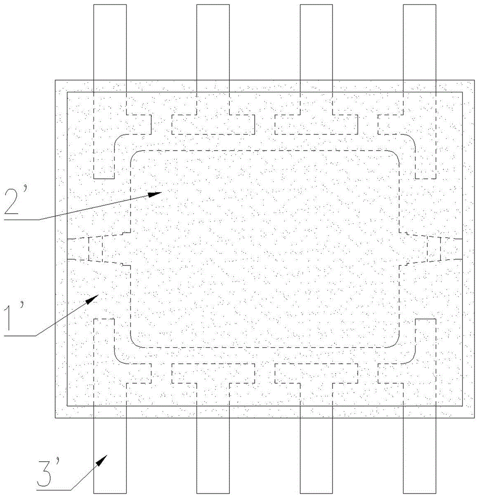
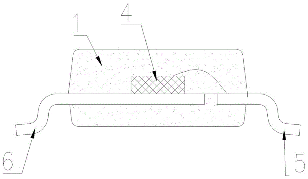
[0021] Such as figure 2 , 3 As shown, the five-pin IC structure proposed by the present invention includes: a plastic package 1, a base island and pins. The base island is composed of an upper base island 2 and a lower base island 3 arranged side by side in the plastic package body 1 up and down. There is a distance between the upper base island 2 and the lower base island 3. There are at least One is equipped with a chip 4, and for products with different structures during production, the chip 4 can be packaged on two base islands at the same time to make a double-chip IC. The two chips 4 are connected inside the plastic package 1 through inner leads, and the IC package The structure is more compact and stable, and the chip 4 can also be packaged on the upper base island 2 or the lower base island 3 to make a single-chip IC.
[0022] The pins are composed of three right pins 5 arranged transversely on the right side of the plastic package 1 and two left pins 6 arranged tra...
PUM
 Abstract
Description
Claims
Application Information
 - R&D
- Intellectual Property
- Life Sciences
- Materials
- Tech Scout
- Unparalleled Data Quality
- Higher Quality Content
- 60% Fewer Hallucinations
Browse by: Latest US Patents, China's latest patents, Technical Efficacy Thesaurus, Application Domain, Technology Topic, Popular Technical Reports.
© 2025 PatSnap. All rights reserved.Legal|Privacy policy|Modern Slavery Act Transparency Statement|Sitemap|About US| Contact US: help@patsnap.com