Organic light-emitting display device, manufacturing method thereof and organic light-emitting display equipment

A light-emitting display device, an organic technology, applied in semiconductor/solid-state device manufacturing, semiconductor devices, electric solid-state devices, etc., can solve the problems of inability to accurately control the position of the light-emitting center, poor device efficiency, etc., to reduce fluorescence quenching phenomenon, improve Effects of luminous efficiency and environmental cost

Active Publication Date: 2017-05-31
WUHAN TIANMA MICRO ELECTRONICS CO LTD +1
View PDF5 Cites 11 Cited by
  • Summary
  • Abstract
  • Description
  • Claims
  • Application Information

AI Technical Summary

Problems solved by technology

[0005] Embodiments of the present invention provide an organic light-emitting display device, a manufacturing method thereof, and an organic light-emitting display device, so as to solve the problems that the existing organic light-emitting display devices cannot accurately control the position of the light-emitting center and the device efficiency is poor

Method used


Image

  • Organic light-emitting display device, manufacturing method thereof and organic light-emitting display equipment
  • Organic light-emitting display device, manufacturing method thereof and organic light-emitting display equipment
  • Organic light-emitting display device, manufacturing method thereof and organic light-emitting display equipment

Examples


Embodiment Construction

[0023] In order to make the purpose, technical solutions and advantages of the present invention clearer, the technical solutions of the present invention will be clearly and completely described through implementation with reference to the accompanying drawings in the embodiments of the present invention. Obviously, the described embodiments are the embodiment of the present invention. Some, but not all, embodiments. Based on the embodiments of the present invention, all other embodiments obtained by persons of ordinary skill in the art without making creative efforts belong to the protection scope of the present invention.

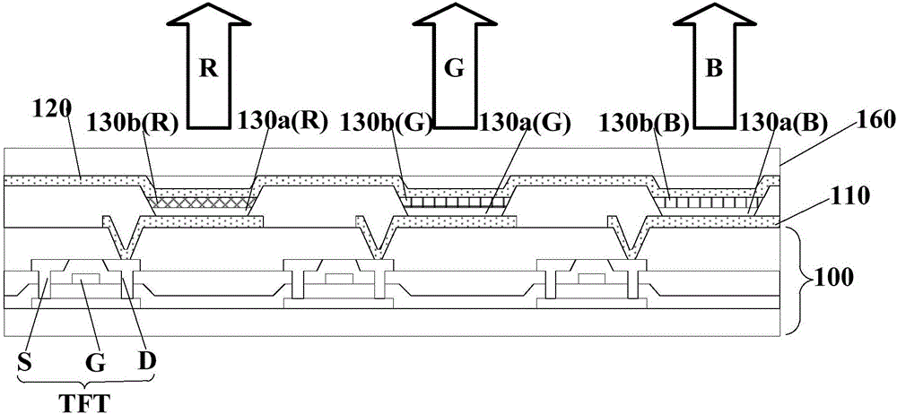
[0024] Such as figure 1 Shown is a schematic diagram of an organic light emitting display provided by an embodiment of the present invention. The organic light emitting display includes a lower substrate 100 and an upper substrate (or thin film encapsulation layer) 160, a TFT (Thin Film Transistor, thin film transistor) array located on the lower substr...


PUM


Abstract

The embodiment of the invention discloses an organic light-emitting display device, a manufacturing method thereof and organic light-emitting display equipment. The organic light-emitting display device comprises a first electrode and a second electrode which are arranged oppositely; a first light-emitting layer and a second light-emitting layer are arranged between the first electrode and the second electrode; the first light-emitting layer is arranged close to the first electrode and is prepared from the composing materials including a first subject material and a first object material; the second light-emitting layer is arranged close to the second electrode and is prepared from the component materials including a second subject material and a heat activation delay fluorescent material. In the embodiment of the invention, the heat activation delay fluorescent material can reduce electron injection obstruction, and an exciplex is difficult to generate; the first light-emitting layer and the second light-emitting layer are arranged, so that a light-emitting center position can be flexibly regulated, the efficiency of the device is improved, and the service life of the device is prolonged; and in addition, the strongest radiation wavelength of the device is fixed after the light-emitting center position is determined, so that the problem that the light color, the brightness and the color error are changed because of offset of the light-emitting center position, is solved.

Description

technical field [0001] Embodiments of the present invention relate to organic light emitting display technologies, and in particular to an organic light emitting display device, a manufacturing method thereof, and an organic light emitting display device. Background technique [0002] Organic light-emitting diode (Organic Light-Emitting Diode, OLED) display device is a self-luminous display device with an organic light-emitting layer located between the cathode and the anode as the illuminant. It has ultra-thin, high brightness, high luminous efficiency and good shock resistance. Advantage. The constituent materials of the organic light-emitting layer usually include a host material and a guest material. After a voltage is applied to the cathode and anode, the triplet exciton energy of the host material is transferred to the triplet exciton energy of the guest material, thereby realizing electroluminescence. [0003] In the organic light-emitting layer of the existing organ...

Claims


Application Information

Patent Timeline
Patent Type & Authority Applications(China)
IPC IPC(8): H01L51/50H01L51/54H01L27/32
CPCH10K59/12H10K50/11H10K2101/40H10K50/13H10K50/12
Inventor 程爽滨田王湘成牛晶华
Owner WUHAN TIANMA MICRO ELECTRONICS CO LTD
Why Eureka
Try Eureka