Pixel compensation circuit, scanning driving circuit and display device

A scanning drive circuit and compensation circuit technology, applied to static indicators, instruments, etc., can solve the problem of uneven brightness display of the panel, and achieve the effect of uniform brightness display of the panel and improvement of threshold voltage deviation

Active Publication Date: 2019-03-15
TCL CHINA STAR OPTOELECTRONICS TECH CO LTD
View PDF4 Cites 0 Cited by
  • Summary
  • Abstract
  • Description
  • Claims
  • Application Information

AI Technical Summary

Problems solved by technology

[0004] The technical problem mainly solved by the present invention is to provide a pixel compensation circuit, a scan drive circuit and a display device to improve the problem of uneven brightness display of the panel caused by the deviation of the threshold voltage

Method used


Image

  • Pixel compensation circuit, scanning driving circuit and display device
  • Pixel compensation circuit, scanning driving circuit and display device
  • Pixel compensation circuit, scanning driving circuit and display device

Examples


Embodiment Construction

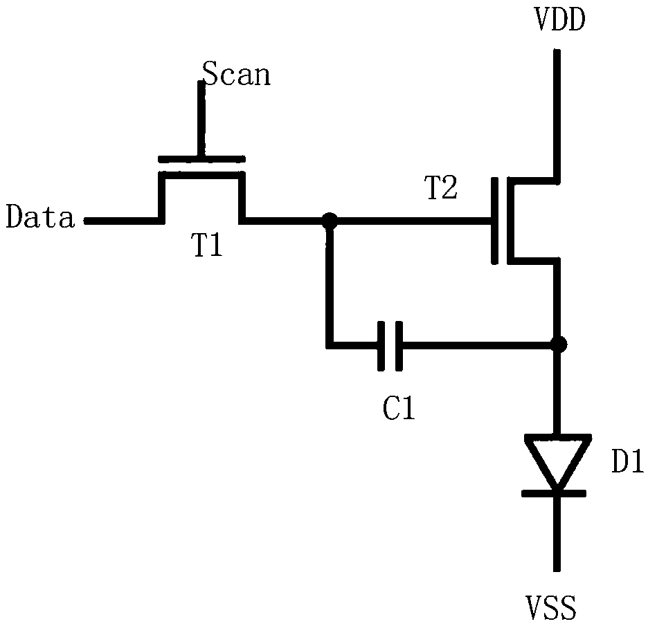
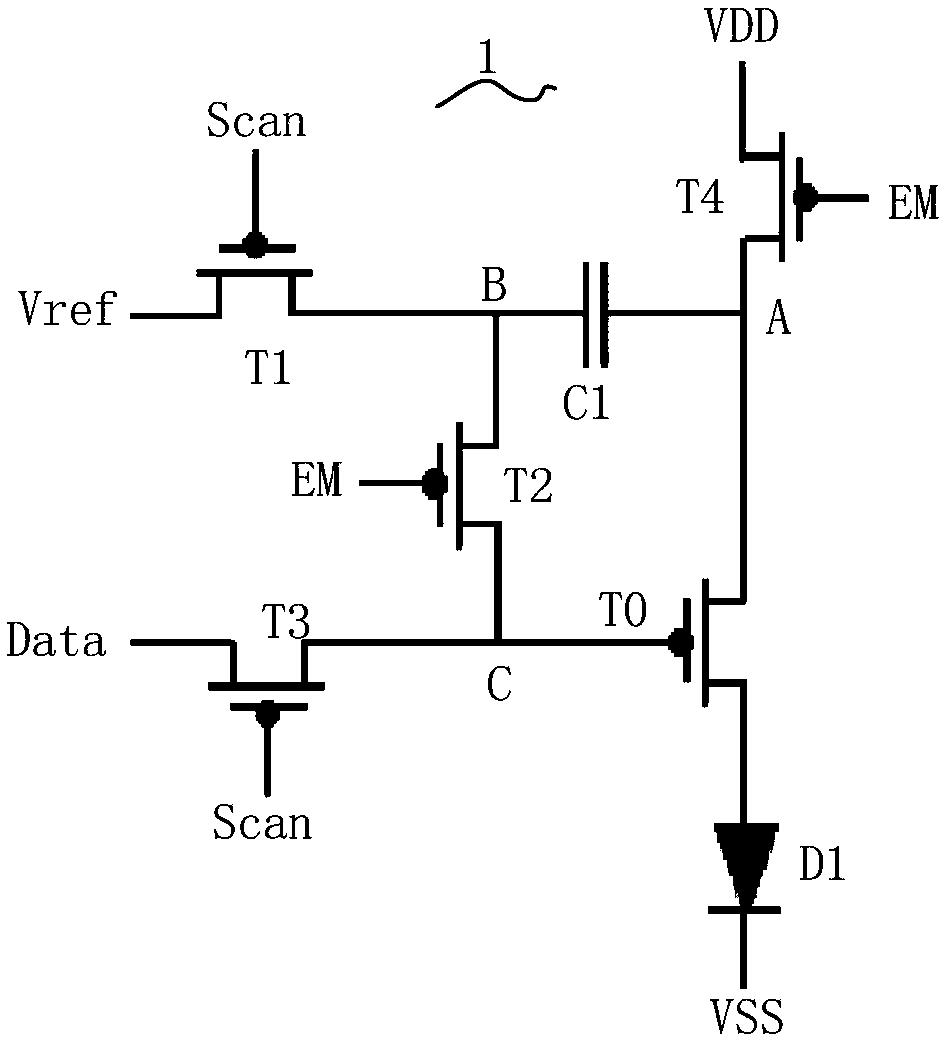
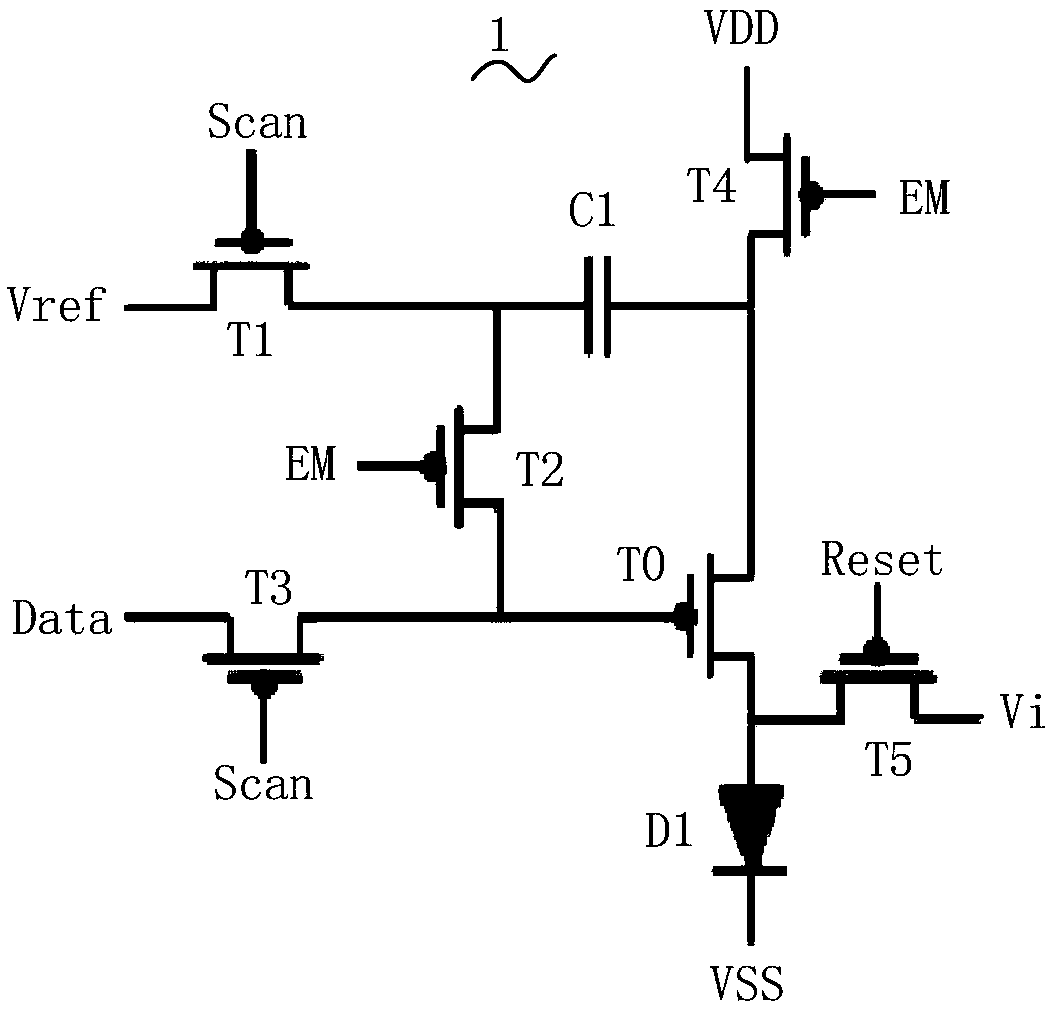
[0030] see figure 2 , is a schematic circuit diagram of the first embodiment of the pixel compensation circuit of the present invention. The pixel compensation circuit includes a first controllable switch T1, the first controllable switch T1 includes a control terminal, a first terminal and a second terminal, the control terminal of the first controllable switch T1 is connected to the scanning line Scan, so The first terminal of the first controllable switch T1 is connected to the reference voltage terminal Vref;

[0031] The second controllable switch T2, the second controllable switch T2 includes a control terminal, a first terminal and a second terminal, the control terminal of the second controllable switch T2 is connected to the light-emitting control terminal EM, and the second controllable switch T2 The first end of the switch T2 is connected to the second end of the first controllable switch T1;

[0032] The third controllable switch T3, the third controllable switc...


PUM


Abstract

Provided are a pixel compensation circuit, a scan driving circuit and a display device. Control ends of the first switch (T1) and the third switch (T3) are connected with a scanning line (Scan). A first end of the first switch (T1) is connected with a reference voltage end (Vref), and a second end thereof is connected with a first end of the second switch (T2). Control ends of the second switch (T2) and the fourth switch (T4) are connected with a light-emitting control end (EM). A first end of the third switch (T3) is connected with a data line (Data), and a second end thereof is connected with a second end of the second switch (T2) and a control end of a driving switch (T0). An anode of a diode (D1) is connected with a second end of the driving switch (T1). A first end of the fourth switch (T4) is connected with a first voltage end (VDD), a second end thereof is connected with a first end of the driving switch (T0). A first end of a storage capacitor (C1) is connected with a second end of the first switch (T1), and a second end thereof is connected with the first end of the driving switch (T0).

Description

technical field [0001] The invention relates to the field of display technology, in particular to a pixel compensation circuit, a scan driving circuit and a display device. Background technique [0002] Due to its wide color gamut, high contrast ratio, solid-state devices and many other excellent features, OLED display devices have been extensively developed in recent years and become more and more competitive in the display field. The current OLED display device basically adopts an active driving method. Since organic light-emitting diodes are current-mode devices, how to precisely control the current has become an important direction of consideration. [0003] The existing pixel compensation circuit is composed of two thin film transistors and a storage capacitor (such as figure 1 As shown), the pixel compensation circuit includes a controllable switch T1, a driving switch T2 and a storage capacitor C1. The driving current of the organic light emitting diode D1 is contro...

Claims


Application Information

Patent Timeline
Patent Type & Authority Patents(China)
IPC IPC(8): G09G3/3258
CPCG09G3/3258
Inventor 李光
Owner TCL CHINA STAR OPTOELECTRONICS TECH CO LTD
Why Eureka
Try Eureka