Liquid crystal display panel and pixel unit thereof

A liquid crystal display panel and pixel unit technology, applied in nonlinear optics, instruments, optics, etc., can solve problems affecting the performance of display devices, etc., and achieve the effect of reducing liquid crystal dumping conflicts and reducing the effect of dark streaks

Active Publication Date: 2017-11-21
SHENZHEN CHINA STAR OPTOELECTRONICS SEMICON DISPLAY TECH CO LTD
View PDF8 Cites 12 Cited by
  • Summary
  • Abstract
  • Description
  • Claims
  • Application Information

AI Technical Summary

Problems solved by technology

[0004] To sum up, due to the pixel structure of the prior art, the liquid crystal in the corresponding area of ​​the cross-shaped main electrode is tilted in the opposite direction, which inevitably produces dark lines, which in turn affects the performance of the display device.

Method used


Image

  • Liquid crystal display panel and pixel unit thereof
  • Liquid crystal display panel and pixel unit thereof
  • Liquid crystal display panel and pixel unit thereof

Examples


Embodiment Construction

[0029] The following descriptions of the various embodiments refer to the accompanying drawings to illustrate specific embodiments in which the invention may be practiced. The directional terms mentioned in the present invention, such as [top], [bottom], [front], [back], [left], [right], [inside], [outside], [side], etc., are only for reference The orientation of the attached schema. Therefore, the directional terms used are used to illustrate and understand the present invention, but not to limit the present invention. In the figures, structurally similar elements are denoted by the same reference numerals.

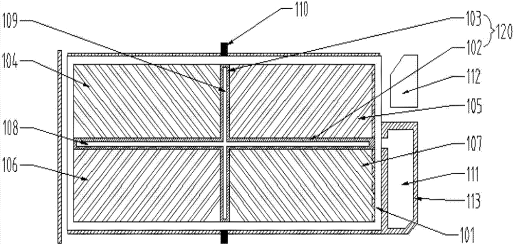
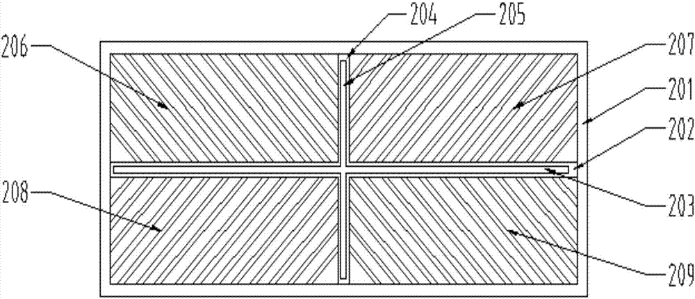
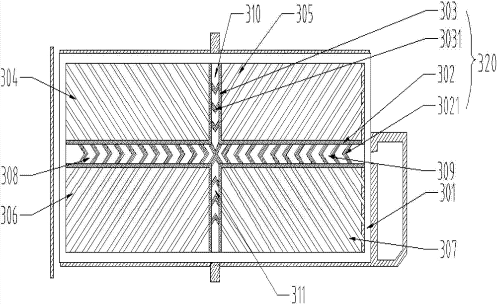
[0030] The present invention is aimed at the pixel structure in the prior art. Since the liquid crystals in the corresponding areas of the cross-shaped backbone electrodes are tilted in opposite directions, dark lines are inevitably generated, which further affects the performance of the display device. This embodiment can solve this defect.

[0031] The liquid crystal...


PUM


Abstract

The invention provides a pixel unit which comprises a peripheral frame, a main electrode and a branch electrode. The peripheral frame encloses a pixel electrode; the main electrode is connected with the peripheral frame and comprises a horizontal main electrode body and a longitudinal main electrode body which are perpendicular to each other in a crisscross manner and divides the pixel electrode into four regions; one end of the branch electrode is connected with the peripheral frame while the other opposite end is connected with the horizontal main electrode body / longitudinal main electrode body; the horizontal main electrode body is provided with a first through hole, the longitudinal main electrode body is provided with a second through hole, the first through hole is connected with the second through hole and enables the main electrode to be a crisscross ring in shape.

Description

technical field [0001] The invention relates to the field of display technology, in particular to a liquid crystal display panel and a pixel unit thereof. Background technique [0002] The HVA (PSVA) mode in liquid crystal display technology is one of many VA modes. The pixel structure of the HVA mode does not need to have bumps, which has great advantages over PVA and MVA, such as reducing the process of bumps, reducing the impact of terrain caused by bumps, and reducing the impact of particles caused by bumps. Wait. [0003] In order to overcome the viewing angle problem of VA mode, ordinary HVA pixel design, like other VA modes, will also be divided into multiple sub-pixel areas (domains) in one pixel area, generally four domains. like Figure 4 Shown is a schematic diagram of the HVA pixel structure in the prior art. The cross-shaped main electrode 401 in the middle of the pixel electrodes is the boundary line between domains and also the place where dark lines are gen...

Claims


Application Information

Patent Timeline
IPC IPC(8): G02F1/1343
CPCG02F1/134309G02F1/134345G02F1/133707G02F1/136209
Inventor 叶岩溪
Owner SHENZHEN CHINA STAR OPTOELECTRONICS SEMICON DISPLAY TECH CO LTD
Why Eureka
Try Eureka