Vacuum absorbing device used for chip testing device

A technology of vacuum adsorption and chip testing, applied in measuring devices, electronic circuit testing, measuring electricity, etc., can solve the problems of increased maintenance man-hours and reduced work efficiency, and achieve the effect of avoiding station height changes

Active Publication Date: 2017-11-28
WUXI CHINA RESOURCE MICRO ASSEMBLY TECH
View PDF16 Cites 5 Cited by
  • Summary
  • Abstract
  • Description
  • Claims
  • Application Information

AI Technical Summary

Problems solved by technology

The existing solution is to regularly check the stickiness of the copper column suction nozzles of all machines every day, and preventive maintenance and cleaning of the copper columns every week, resulting in increased maintenance hours and reduced work efficiency

Method used


Image

  • Vacuum absorbing device used for chip testing device
  • Vacuum absorbing device used for chip testing device
  • Vacuum absorbing device used for chip testing device

Examples


Embodiment Construction

[0021] In order to make the above objects, features and advantages of the present invention more comprehensible, the present invention will be further described in detail below in conjunction with the accompanying drawings and specific embodiments.

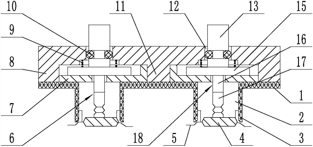
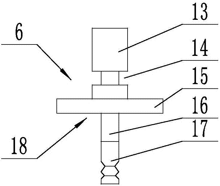
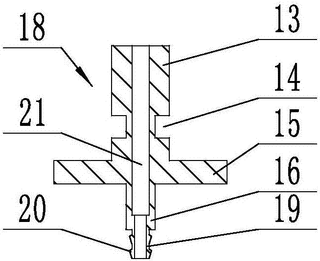
[0022] Such as figure 1 As shown, the present invention is a vacuum adsorption device, which is used to adsorb chips 4 in chip testing equipment, which includes a base body 8 and a cover plate 1 fixed together.

[0023] The outer surface of the cover plate 1 is provided with an outwardly protruding chip pin support wall 3 , and the chip pin support wall 3 is used to support the chip pins 5 of the chip 4 to be tested. Chip accommodating cavities 2 are formed between the chip lead support walls 3, and there may be one or more chip accommodating cavities, two in this embodiment.

[0024] The base body 8 is provided with through holes 12 corresponding to the positions of the chip receiving chambers 2; the number of the through holes ...


PUM


Abstract

The invention relates to a vacuum absorbing device used for a chip testing device. The vacuum absorbing device comprises a seat body and a cover plate; chip pin support walls projecting out are arranged on the outer surface of the cover plate; chip containing cavities are formed between the chip pin support walls; through holes corresponding to the positions of the chip containing cavities are formed in the seat body; suction nozzle partss are installed between the through holes of the seat body and the chip containing cavities of the cover plate; the suction nozzle part comprises a suction nozzle column body and a rubber suction nozzle; an axial-through air hole is formed in the suction nozzle column body; one end of the suction nozzle column body is projected out of the through hole of the seat body; the other end of the suction nozzle column body is fixed with the rubber suction nozzle; the rubber suction nozzle is communicated with the air hole; the rubber suction nozzle is arranged inside the chip containing cavity; and a spring sleeves the columnar surface of the suction nozzle column body. The telescopic rubber suction nozzle is arranged on the suction nozzlepart, which can effectively avoid the change of a standing height due to a fact that the pin of the chip is under pressure.

Description

technical field [0001] The invention relates to testing equipment for integrated circuit chips, in particular to a vacuum adsorption device for chip testing equipment. Background technique [0002] When the integrated circuit chip is tested on the test equipment, a vacuum adsorption device is often used to pick and place the chip. [0003] The existing vacuum adsorption device includes a seat body and a cover plate fixed together, and the seat body is installed on the test equipment. The outer surface of the cover plate is provided with an outwardly protruding chip accommodating cavity, the outer end of the chip accommodating cavity is provided with a chip pin supporting wall, and the seat body is provided with a through hole corresponding to the accommodating cavity. The copper column suction nozzle is installed between the base body and the cover plate, and an intermediate cylinder is arranged in the middle of the copper column suction nozzle. One end of the copper colum...

Claims


Application Information

Patent Timeline
Patent Type & Authority Applications(China)
IPC IPC(8): G01R31/28
CPCG01R31/2851
Inventor 柳继营赵丹黄海军
Owner WUXI CHINA RESOURCE MICRO ASSEMBLY TECH
Why Eureka
Try Eureka