
Display panel and display device

A display panel and display device technology, which is applied in the direction of instruments, nonlinear optics, optics, etc., can solve the problems of insufficient charging of the panel, poor display effect of high-resolution display panels, etc., so as to improve the display effect and reduce the problem of block boundaries Generates, doubles the charging time

Active Publication Date: 2020-12-25
SHENZHEN CHINA STAR OPTOELECTRONICS SEMICON DISPLAY TECH CO LTD
View PDF3 Cites 0 Cited by
  • Summary
  • Abstract
  • Description
  • Claims
  • Application Information

AI Technical Summary

Problems solved by technology

[0003] The technical problem mainly solved by this application is to provide a display panel and a display device, which are used to solve the problems of poor display effect of high-resolution display panels and insufficient charging of the panel in the prior art

Method used


Image

  • Display panel and display device
  • Display panel and display device
  • Display panel and display device

Examples


Embodiment Construction

[0023] The following will clearly and completely describe the technical solutions in the embodiments of the present application. Obviously, the described embodiments are only some of the embodiments of the present application, rather than all the embodiments. Based on the embodiments in this application, all other embodiments obtained by persons of ordinary skill in the art without making creative efforts belong to the scope of protection of this application.

[0024] The terms "first" and "second" in this application are only used for descriptive purposes, and should not be understood as indicating or implying relative importance or implicitly specifying the quantity of indicated technical features. Thus, the features defined as "first" and "second" may explicitly or implicitly include at least one of these features. In the description of the present application, "plurality" means at least two, such as two, three, etc., unless otherwise specifically defined. All directional ...


PUM


Abstract

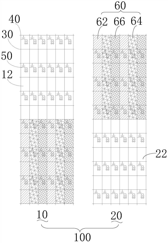
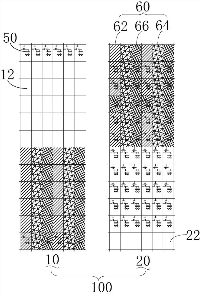
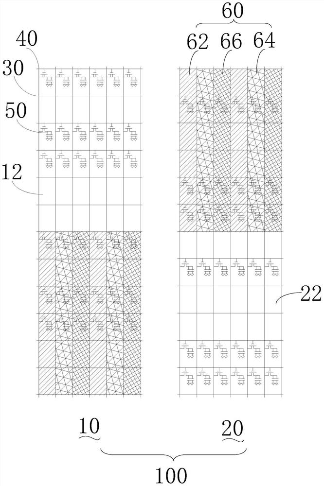
A display panel (1000). The display panel (1000) comprises: a first substrate (10); a second substrate (20); first gate lines (110) and first data lines (120) provided at the first substrate (10); and second gate lines (210) and second data lines (220) provided at the second substrate (20). The first gate lines (110) and the first data lines (120) enclose a first pixel region (140). The second gate lines (210) and the second data lines (220) enclose a second pixel region (240). A projection of the first pixel region (140) in which a first thin film transistor (130) is provided is located between two second pixel regions (240) corresponding to at least two adjacent second thin film transistors (230). The invention increases charging efficiency and reduces block boundary lines, thereby improving display performance.

Description

technical field [0001] The present application relates to the field of display technology, in particular to a display panel and a display device. Background technique [0002] With the development of display panel technology, higher and higher resolutions (such as 4K, 2K; 8K, 4K; 16K, 8K) have become the technical goals that people pursue. Increase, the increased charging index, that is, RC (R represents the resistance value, C represents the capacitance value) will make the color displayed on the panel uneven; at the same time, the increase in resolution will also lead to a sharp decrease in charging time, for example: when the frequency remains unchanged In the case of 2K, 1K charging time is t, 4K, 2K charging time is t / 2, 8K, 4K charging time is t / 4, 16K, 8K charging time is t / 8, insufficient charging will affect Displays the transmittance of the panel. Due to the superposition of these factors, the display effect of the liquid crystal panel and the transmittance of th...

Claims


Application Information

Patent Timeline
Patent Type & Authority Patents(China)
IPC IPC(8): G02F1/1362G02F1/1335
CPCG02F1/133514G02F1/1362G02F1/136222
Inventor 何文超
Owner SHENZHEN CHINA STAR OPTOELECTRONICS SEMICON DISPLAY TECH CO LTD
Learn More