Ion implantation method

A technology of ion implantation and ion implanter, which is applied in the manufacture of electrical components, semiconductor/solid-state devices, circuits, etc., and can solve problems such as uncontrollable metal pollution, poor test stability, and impact on film quality

Active Publication Date: 2019-02-01
SHANGHAI HUALI INTEGRATED CIRCUTE MFG CO LTD
View PDF5 Cites 0 Cited by
  • Summary
  • Abstract
  • Description
  • Claims
  • Application Information

AI Technical Summary

Problems solved by technology

[0006] At present, the ion implanter usually monitors the metal molybdenum by measuring the metal content of the control chip through an inductively coupled plasma analyzer (ICPMS). The ICPMS test has long test time, high cost, easy to be affected by the quality of the control chip, and test stability. Poor and unable to control metal contamination

Method used


Image

  • Ion implantation method
  • Ion implantation method
  • Ion implantation method

Examples


Embodiment Construction

[0022] The technical solutions of the present invention will be clearly and completely described below with reference to the accompanying drawings. Obviously, the described embodiments are a part of the embodiments of the present invention, but not all of the embodiments. Based on the embodiments of the present invention, all other embodiments obtained by those of ordinary skill in the art without creative work fall within the protection scope of the present invention.

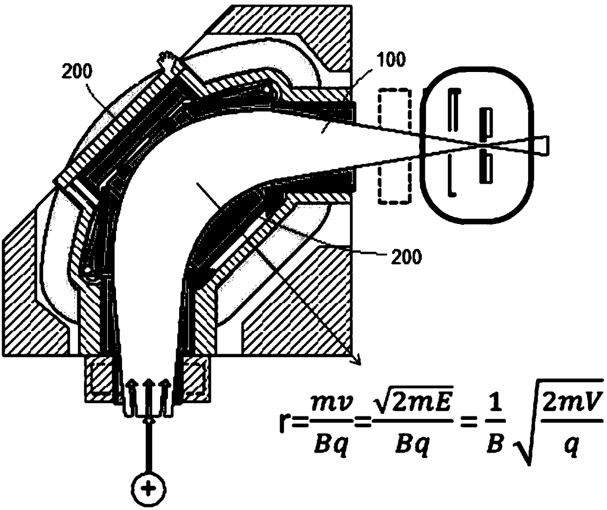
[0023] In an embodiment of the present invention, an ion implantation method is provided, which includes: using an isotope ion source gas BF3 composed of boron isotopes and / or fluorine isotopes as an ion source of an ion implanter, and the ion implanter injects the isotope ion source gas BF3 is ionized to form BF2+ doping ions, wherein the difference between the equivalent mass-to-charge ratio of BF2+ doping ions and the equivalent mass-to-charge ratio of molybdenum metal Mo2+ is not less than 1.

[0024] The ...


PUM


Abstract

The invention relates to an ion implantation method, and relates to semiconductor integrated circuit manufacture technologies. Isotope ion source gas BF3 composed of isotope of boron and/or isotope offluorine serves as an ion source of an ion implantation device, the ion implantation device ionized the isotope ion source gas BF3 to form BF2+ doped ions, the equivalent mass-to-charge ratio of theBF2+ doped ions is increased or decreased, thus, when the exciting current of a magnetic field during adjustment and analyzes equals a first current, the BF2+ doped ions are easier to separate from molybdenum Mo2+, and when the doped ions are implanted into a wafer, pollution caused by Mo2+ can be avoided.

Description

technical field [0001] The present invention relates to semiconductor integrated circuit manufacturing technology, in particular to an ion implantation method. Background technique [0002] In the semiconductor integrated circuit manufacturing technology, the doping process of introducing specified impurities into the semiconductor is one of the key steps. The doping process includes a diffusion process and an ion implantation process, wherein the diffusion process is gradually replaced by the ion implantation process due to poor doping control and the generation of dislocations on the wafer surface. The ion implantation process allows for better control over the location and amount of doping within the wafer. During the ion implantation process, the ion source gas is ionized, separated, and accelerated (gaining kinetic energy) to form a doped ion beam that sweeps across the wafer. The dopant ions physically bombard the wafer, producing a Gaussian distribution on the wafer...

Claims


Application Information

Patent Timeline
Patent Type & Authority Applications(China)
IPC IPC(8): H01L21/265
CPCH01L21/265
Inventor 伍菲菲时锋袁立军
Owner SHANGHAI HUALI INTEGRATED CIRCUTE MFG CO LTD
Why Eureka
Try Eureka