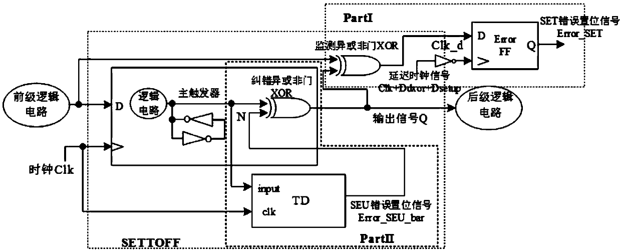
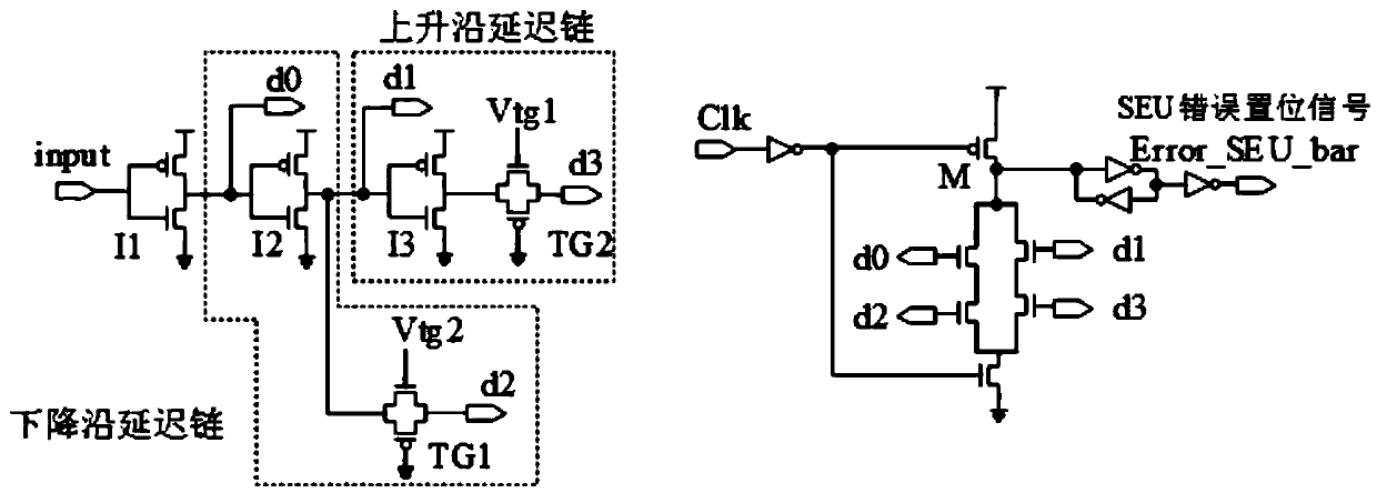
An edge detection circuit for monitoring whether a trigger is overturned or not and the trigger
An edge detection and trigger technology, which is applied in the direction of instruments, static memory, digital memory information, etc., can solve the problems of increasing the input and output propagation delay of TD circuits, glitch pulse pipeline rewriting operations, etc., and achieve the effect of small area
- Summary
- Abstract
- Description
- Claims
- Application Information
AI Technical Summary
Problems solved by technology
Method used
Image

Examples
specific Embodiment approach 1
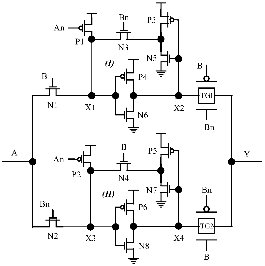
[0021] Embodiment 1: An edge detection circuit for monitoring flip-flops in this embodiment is composed of 6 PMOS transistors, 8 NMOS transistors and two transmission gates;
[0022] Wherein, the 6 PMOS transistors are respectively PMOS transistors P1 to P6; the 8 NMOS transistors are respectively N1 to N8; the transmission gates are TG1 and TG2; both TG1 and TG2 are composed of an NMOS transistor and a PMOS transistor;
[0023]The drain of PMOS transistor P1 is connected to node X1, its gate is connected to node An, and its source is connected to the power supply; the drain of PMOS transistor P2 is connected to node X3, its gate is connected to node An, and its source is connected to Power supply; the drain of PMOS transistor P3 is connected to the source of NMOS transistor N3, its gate is connected to node X2, and its source is connected to the power supply; the drain of PMOS transistor P4 is connected to node X2, and its gate is connected to node X1 , its source is connecte...
specific Embodiment approach 2
[0024] Specific embodiment 2: The difference between this embodiment and specific embodiment 1 is that the input signal is input by node A; the input signal is divided into two paths to form feedback loops I and II, and the high voltage of the clock signal is transmitted through transmission gates TG1 and TG2 respectively. The flat period and the low period alternately act on node Y; the feedback loop I is composed of a pre-charged PMOS transistor P1, a single-transistor transmission transistor N3 and two inverters, of which the two inverters are respectively composed of transistors P3 and N5 and P4 and N6; the feedback loop II is composed of a pre-charged PMOS transistor P2, a single-transistor transfer transistor N4 and two inverters, of which the two inverters are composed of transistors P5 and N7, and P6 and N8. Others are the same as in the first embodiment.
specific Embodiment approach 3
[0025] Embodiment 3: The difference between this embodiment and Embodiment 1 is that both feedback loops I and II include a pre-charge transistor, a transfer transistor and two inverters; wherein, the pre-charge transistor is P1 or P2, transfer pipe is N3 or N4. Others are the same as in the first embodiment.
PUM
 Abstract
Description
Claims
Application Information
PatSnap Eureka turns technology decisions into work you can execute. Powered by our Innovation Knowledge Graph, it runs expert workflows across engineering, life sciences, materials and intellectual property. Get your review-ready output in minutes.


