Check patentability & draft patents in minutes with Patsnap Eureka AI!

An edge detection circuit and flip-flop for monitoring flip-flop occurrence

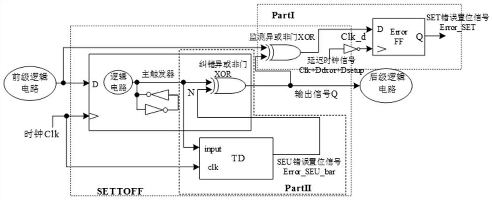
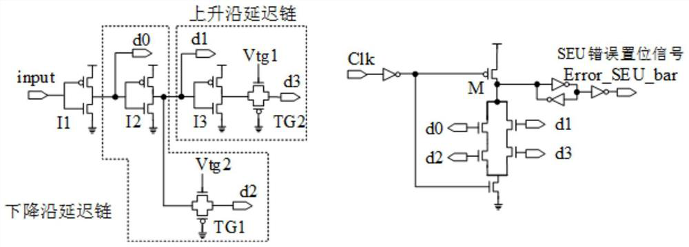
An edge detection and trigger technology, applied in the direction of instruments, static memory, digital memory information, etc., can solve problems such as glitch pulse pipeline rewriting operation, increase TD circuit input and output propagation delay, etc., to reduce error correction glitches Effect of pulse width, small area

Inactive Publication Date: 2021-06-01
HARBIN INST OF TECH
View PDF2 Cites 0 Cited by
  • Summary
  • Abstract
  • Description
  • Claims
  • Application Information

AI Technical Summary

Problems solved by technology

[0005] The purpose of the present invention is to solve the online monitoring and correction of SEU soft errors by SETTOFF flip-flops and the process of detecting SET and TE errors. The transistor size in the TD circuit cannot be realized with the minimum size and must be specially designed, thereby increasing The propagation delay between the input and output of the TD circuit is increased, and then glitch pulses are generated to cause the problem of rewriting operations of the pipeline

Method used


Image

  • An edge detection circuit and flip-flop for monitoring flip-flop occurrence
  • An edge detection circuit and flip-flop for monitoring flip-flop occurrence
  • An edge detection circuit and flip-flop for monitoring flip-flop occurrence

Examples


specific Embodiment approach 1

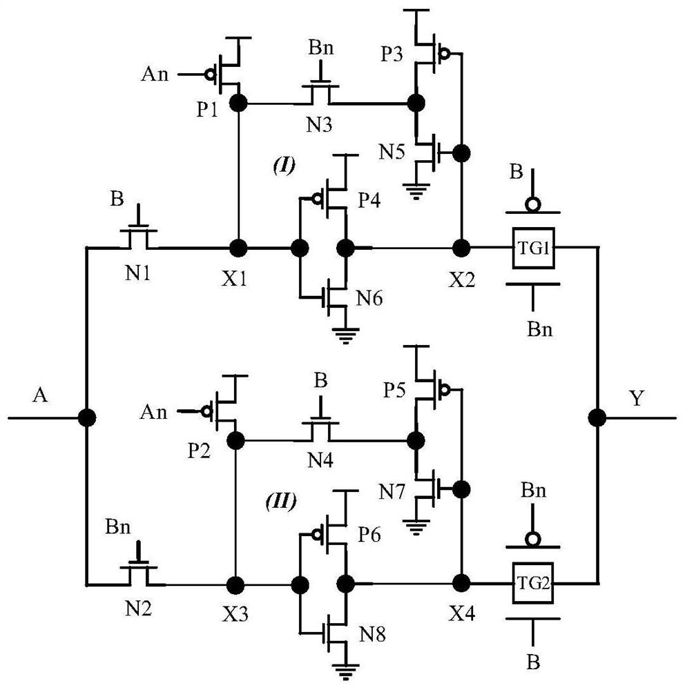
[0021] Specific Embodiment 1: An edge detection circuit for monitoring flip-flops in this embodiment is composed of 6 PMOS transistors, 8 NMOS transistors and two transmission gates;

[0022] Wherein, the 6 PMOS transistors are respectively PMOS transistors P1 to P6; the 8 NMOS transistors are respectively N1 to N8; the transmission gates are TG1 and TG2; both TG1 and TG2 are composed of an NMOS transistor and a PMOS transistor;

[0023]The drain of PMOS transistor P1 is connected to node X1, its gate is connected to node An, and its source is connected to the power supply; the drain of PMOS transistor P2 is connected to node X3, its gate is connected to node An, and its source is connected to Power supply; the drain of PMOS transistor P3 is connected to the source of NMOS transistor N3, its gate is connected to node X2, and its source is connected to the power supply; the drain of PMOS transistor P4 is connected to node X2, and its gate is connected to node X1 , its source is...

specific Embodiment approach 2

[0024] Specific embodiment 2: The difference between this embodiment and specific embodiment 1 is that the input signal is input by node A; the input signal is divided into two paths to form feedback loops I and II, and the high voltage of the clock signal is transmitted through transmission gates TG1 and TG2 respectively. The flat period and the low period alternately act on node Y; the feedback loop I is composed of a pre-charged PMOS transistor P1, a single-transistor transmission transistor N3 and two inverters, of which the two inverters are respectively composed of transistors P3 and N5 and P4 and N6; the feedback loop II is composed of a pre-charged PMOS transistor P2, a single-transistor transfer transistor N4 and two inverters, of which the two inverters are composed of transistors P5 and N7, and P6 and N8. Others are the same as in the first embodiment.

specific Embodiment approach 3

[0025] Embodiment 3: The difference between this embodiment and Embodiment 1 is that both feedback loops I and II include a pre-charge transistor, a transfer transistor and two inverters; wherein, the pre-charge transistor is P1 or P2, transfer pipe is N3 or N4. Others are the same as in the first embodiment.


PUM


Abstract

An edge detection circuit and a trigger for monitoring whether flip-flops occur, which relate to an edge detection circuit and a trigger. The present invention solves the problem that the transistor size in the original edge detection (TD) circuit in the SETTOFF flip-flop cannot be realized with the minimum size but must go through a special The design of the TD circuit increases the propagation delay between the input and output of the TD circuit, and then generates a glitch pulse that causes the rewriting operation of the pipeline. The invention designs an edge detection circuit for monitoring whether flip-flops in the pipeline occur, and realizes the monitoring and correction of the single-event flip-flop effect of the D flip-flop as well as the single-event transient effect and timing errors through a reasonable monitoring mechanism The monitoring function of the invention is applied to the trigger field.

Description

technical field [0001] The invention relates to the field of edge detection circuits and flip-flops, in particular to an edge detection circuit and a flip-flop for monitoring whether a flip-flop in a pipeline is reversed. Background technique [0002] As process geometries continue to shrink, soft errors caused by radiation effects are becoming more and more serious. When high-energy particles bombard a certain node of the storage unit, the storage state of the node will be reversed, thereby inducing the reversal of the entire storage unit, which is the so-called Single Event Upset (SEU). For the SEU that occurs on the SRAM memory, it can be protected by Error Correction Codes (ECC). However, the SEU that occurs in the flip-flop is difficult to correct with the ECC method, because the flip-flop is widely used. Distributed throughout the system-on-a-chip. [0003] In order to make SEU fault-tolerant, so far, researchers have proposed various types of radiation-hardened flip...

Claims


Application Information

Patent Timeline
Patent Type & Authority Patents(China)
IPC IPC(8): G11C7/24G11C11/413
CPCG11C7/24G11C11/413
Inventor 王天琦刘超铭齐春华马国亮张延清霍明学肖立伊
Owner HARBIN INST OF TECH
Features
  • R&D
  • Intellectual Property
  • Life Sciences
  • Materials
  • Tech Scout
  • Unparalleled Data Quality
  • Higher Quality Content
  • 60% Fewer Hallucinations
Learn More