A kind of perovskite thin film solar cell and preparation method thereof
A solar cell and perovskite technology, applied in the field of solar cells, can solve problems such as complex structures and processes, different structures, and high equipment costs, and achieve good film density, improved repeatability, and low deposition temperature.
- Summary
- Abstract
- Description
- Claims
- Application Information
AI Technical Summary
Problems solved by technology
Method used
Image


Examples
Embodiment 1
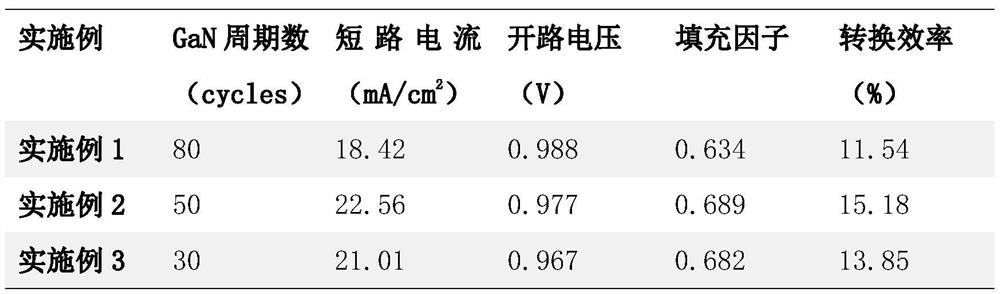
[0066] First, put the FTO conductive glass into the reaction chamber of the PEALD system and evacuate it to ~0.15 Torr, then raise the temperature to 240°C and keep it for 30 minutes to stabilize the temperature. GaN was deposited using high-purity N 2 、H 2 and Ar(N 2 :H 2 :Ar=3:6:1) mixed plasma and triethylgallium as precursor, high-purity Ar as purge gas. The deposition of GaN needs to be completed in sequence: the plasma is injected for 30s and then purged for 30s, followed by TEG for 0.5s and reacted for 45s and then purged for 30s. The preparation of atomic layer deposition GaN thin film electron transport layer requires 80 cycles (cycles), and the thickness is about 8nm. Next, MAPbI was prepared by one-step spin-coating on the surface of atomic layer deposition GaN thin film electron transport layer. 3 Perovskite light-absorbing layer, first configure MAPbI 3 Reaction precursor solution: Weigh 0.578g PbI and 0.2g MAI respectively, add to 1mL DMF, stir at room temp...
Embodiment 2
[0071]First, put the FTO conductive glass into the reaction chamber of the PEALD system and evacuate it to ~0.15 Torr, then raise the temperature to 280°C and keep it for 30min to stabilize the temperature. GaN was deposited using high-purity N 2 、H 2 and Ar(N 2 :H 2 :Ar=3:6:1) mixed plasma and triethylgallium as precursor, high-purity Ar as purge gas. The deposition of GaN needs to be completed in sequence: the plasma is injected for 30s and then purged for 30s, followed by TEG for 0.5s and reacted for 45s and then purged for 30s. The preparation of atomic layer deposition GaN thin film electron transport layer requires 50 cycles, and the thickness is about 5nm. Next, MAPbI was prepared by one-step spin-coating on the surface of atomic layer deposition GaN thin film electron transport layer. 3 Perovskite light-absorbing layer, first configure MAPbI 3 Reaction precursor solution: Weigh 0.578g PbI and 0.2g MAI respectively, add to 1mL DMF, stir at room temperature for 1h ...
Embodiment 3
[0076] First, put the FTO conductive glass into the reaction chamber of the PEALD system and evacuate it to ~0.15 Torr, then raise the temperature to 280°C and keep it for 30min to stabilize the temperature. GaN was deposited using high-purity N 2 、H 2 and Ar(N 2 :H 2 :Ar=3:6:1) mixed plasma and triethylgallium as precursor, high-purity Ar as purge gas. The deposition of GaN needs to be completed in order: the plasma is injected for 30s and then purged for 30s, followed by TMG for 0.5s and reacted for 45s and then purged for 30s. The preparation of atomic layer deposition GaN thin film electron transport layer requires 30 cycles, and the thickness is about 3nm. Next, MAPbI was prepared by one-step spin-coating on the surface of atomic layer deposition GaN thin film electron transport layer. 3 Perovskite light-absorbing layer, first configure MAPbI 3 Reaction precursor solution: Weigh 0.578g PbI and 0.2g MAI respectively, add to 1mL DMF, stir at room temperature for 1h to...
PUM
| Property | Measurement | Unit |
|---|---|---|
| thickness | aaaaa | aaaaa |
| thickness | aaaaa | aaaaa |
| thickness | aaaaa | aaaaa |
Abstract
Description
Claims
Application Information
 - R&D
- Intellectual Property
- Life Sciences
- Materials
- Tech Scout
- Unparalleled Data Quality
- Higher Quality Content
- 60% Fewer Hallucinations
Browse by: Latest US Patents, China's latest patents, Technical Efficacy Thesaurus, Application Domain, Technology Topic, Popular Technical Reports.
© 2025 PatSnap. All rights reserved.Legal|Privacy policy|Modern Slavery Act Transparency Statement|Sitemap|About US| Contact US: help@patsnap.com