FPGA, dual-screen TV, boot display method, device and medium
A technology to display and image, applied in FPGA, equipment and media, power-on display method, dual-screen TV field, can solve problems such as image signal instability, blurred screen, black screen, etc., and achieve the effect of avoiding black screen problems
- Summary
- Abstract
- Description
- Claims
- Application Information
AI Technical Summary
Problems solved by technology
Method used
Image
Examples
Embodiment 1
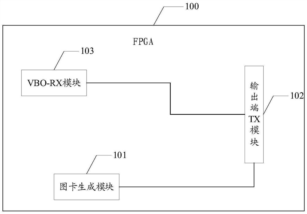
[0061] figure 1 A schematic structural diagram of an FPGA provided by an embodiment of the present invention, such as figure 1 As shown, the FPGA 100 includes: a graphic card generation module 101, an output TX module 102 and a VBO-RX module 103;
[0062] The VBO-RX module 103 is used to send the first signal to the MCU 200 when it does not receive a stable image signal;
[0063] The image card generation module 101 is configured to receive a start command sent by the MCU 200 after receiving the first signal, and generate a LOGO image to be displayed on the lower panel according to the image card information of the pre-saved LOGO image, wherein, The card information includes light transmittance information;
[0064] The output end TX module 102 is configured to receive the LOGO image to be displayed on the lower panel, and send the LOGO image to the lower panel for display.
[0065] In this embodiment of the present invention, the FPGA 100 includes a graphic card generation...
Embodiment 2
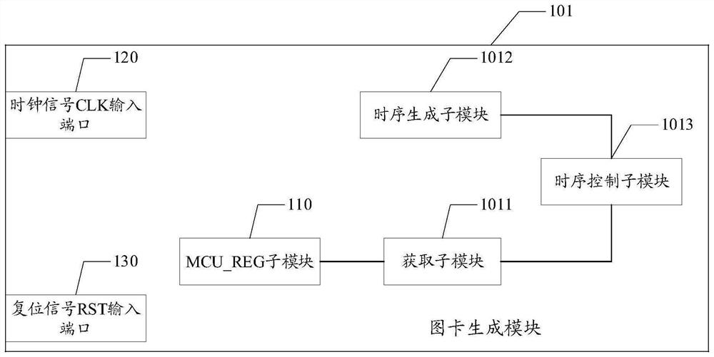
[0084] In order to display the LOGO image more accurately, on the basis of the above embodiment, in this embodiment of the present invention, the image card generation module 101 includes:
[0085] The obtaining sub-module 1011 is configured to obtain the image card information of the pre-saved LOGO image after receiving the startup command sent by the MCU 200, and send the image card information to the timing control sub-module 1013;
[0086] The timing generation sub-module 1012 is configured to generate a first timing signal for controlling the display of the LOGO image according to the received clock signal sent by the MCU, and send the first timing signal to the timing control sub-module 1013 ;
[0087]The timing control sub-module 1013 is configured to determine each target moment for displaying the LOGO image according to the received first timing signal, and at each target moment, the lower panel generated according to the image card information The LOGO image to be d...
Embodiment 3
[0102] In order to establish a stable connection between the VBO-RX module 103 and the image signal, on the basis of the above-mentioned embodiments, in this embodiment of the present invention, the VBO-RX module 103 is also used for receiving the first data sent by the MCU 200. When there is a control signal, the VBO-RX module 103 is controlled to reset, wherein the first control signal is sent by the MCU after receiving the first signal.
[0103] In this embodiment of the present invention, the VBO-RX module 103 resets after receiving the first control signal sent by the MCU 200 , where the first control signal is generated after the MCU 200 receives the first signal.
[0104] In the embodiment of the present invention, after the FPGA 100 loads the netlist file, the MCU 200 configures parameters for the VBO-RX module 103 in the FPGA 100, and after a reset, the VBO-RX module 103 starts to establish a connection with the image signal.
[0105] In order to reset itself when the...
PUM
 Abstract
Description
Claims
Application Information


