Display device and preparation method thereof

A technology for display devices and wavelength conversion layers, applied in semiconductor devices, electric solid state devices, electrical components, etc., can solve the problems of light leakage, reduced conversion efficiency, low yield, etc., and achieve tight integration, improved efficiency, and high light source conversion efficiency. Effect

Pending Publication Date: 2022-05-27
RAYSOLVE OPTOELECTRONICS (SUZHOU) CO LTD
View PDF0 Cites 1 Cited by
  • Summary
  • Abstract
  • Description
  • Claims
  • Application Information

AI Technical Summary

Problems solved by technology

The color conversion layer can be integrated into the display substrate by means of transfer, but it involves the transfer of conversion layers of multiple colors. The traditional one-time overall transfer method has a low yield rate. At the same time, the thickness of different color conversion layers is not uniform, which will lead to One or several color conversion layers are not tightly bonded to the display substrate, causing light leakage and reducing conversion efficiency, resulting in poor display effect

Method used


Image

  • Display device and preparation method thereof
  • Display device and preparation method thereof
  • Display device and preparation method thereof

Examples


Embodiment Construction

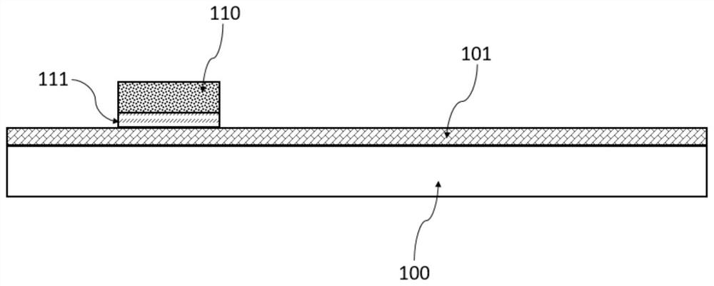
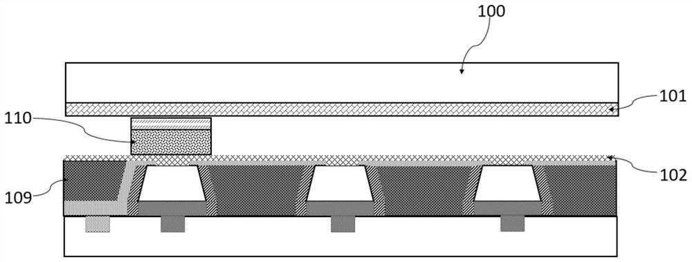
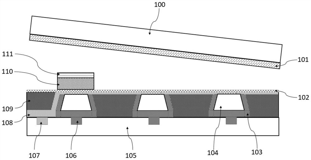
[0079] The technical solutions in the embodiments of the present invention will be clearly and completely described below with reference to the accompanying drawings in the embodiments of the present invention. Obviously, the described embodiments are only some, but not all, embodiments of the present invention. Based on the embodiments of the present invention, all other embodiments obtained by those skilled in the art without creative efforts shall fall within the protection scope of the present invention.

[0080] The present disclosure provides many different embodiments or examples for implementing different structures of the present invention. In order to simplify the present disclosure, specific example components and arrangements are described herein. Of course, they are only examples and are not intended to limit the invention. Furthermore, the present disclosure may repeat reference numerals and / or reference letters in different instances for the purpose of simplic...


PUM

PropertyMeasurementUnit
thicknessaaaaaaaaaa
thicknessaaaaaaaaaa
thicknessaaaaaaaaaa

Abstract

The invention discloses a display device and a preparation method thereof, and belongs to the technical field of semiconductor devices.The preparation method of the display device comprises the steps that wavelength conversion layers are provided, and the wavelength conversion layers comprise the first wavelength conversion layer and the second wavelength conversion layer which are provided respectively; the thickness of the second wavelength conversion layer is greater than that of the first wavelength conversion layer; the first wavelength conversion layer is firstly transferred to a pixel point through the substrate, and then the second wavelength conversion layer is transferred to other pixel points through the substrate; according to the invention, the wavelength conversion layer and the wavelength conversion layer transferred according to the thickness sequence are respectively provided, so that the preparation of the display device for transferring the wavelength conversion layer according to the sequence is realized. The display device provided by the invention comprises at least two wavelength conversion layers with different thicknesses, so that no gap exists between the wavelength conversion layers and the pixel points, and the combination is tighter.

Description

technical field [0001] The invention belongs to the technical field of semiconductor devices, in particular to a display device and a preparation method thereof. Background technique [0002] Micro-display (Micro-LED, micro light-emitting diode) is realized by LED miniaturization and matrixing. Compared with traditional LED display, Micro-LED is different in die, packaging, integration process, backplane, driver and other processes. [0003] Micro-LED, also known as micro light-emitting diode, refers to a high-density integrated LED array. The distance between the LED pixels in the array is in the order of 0.1-100 microns, and each LED pixel can emit light by itself. Since a higher number of integrations can be obtained on a chip of the same area, the integration density of Micro-LED microdisplays is greatly improved, thereby increasing the display resolution, while ensuring high brightness, and can achieve low energy consumption or high brightness display design. [0004] ...

Claims


Application Information

Patent Timeline
Patent Type & Authority Applications(China)
IPC IPC(8): H01L27/15H01L33/50
CPCH01L27/156H01L33/505H01L33/508H01L2933/0041
Inventor 仉旭庄永漳
Owner RAYSOLVE OPTOELECTRONICS (SUZHOU) CO LTD
Why Eureka
Try Eureka