Lateral field effect transistor of sic, method for production thereof and a use of such a transistor

A technology of field-effect transistors and transistors, applied in semiconductor/solid-state device manufacturing, semiconductor devices, electrical components, etc., can solve the problem of not fully utilizing materials

Inactive Publication Date: 2002-03-06
クレースウェーデンアクチボラゲット
View PDF1 Cites 3 Cited by
  • Summary
  • Abstract
  • Description
  • Claims
  • Application Information

AI Technical Summary

Problems solved by technology

The value of the gate length that can be obtained with currently available pattern determination tools is significantly lower than the

Method used


Image

  • Lateral field effect transistor of sic, method for production thereof and a use of such a transistor
  • Lateral field effect transistor of sic, method for production thereof and a use of such a transistor
  • Lateral field effect transistor of sic, method for production thereof and a use of such a transistor

Examples


Embodiment Construction

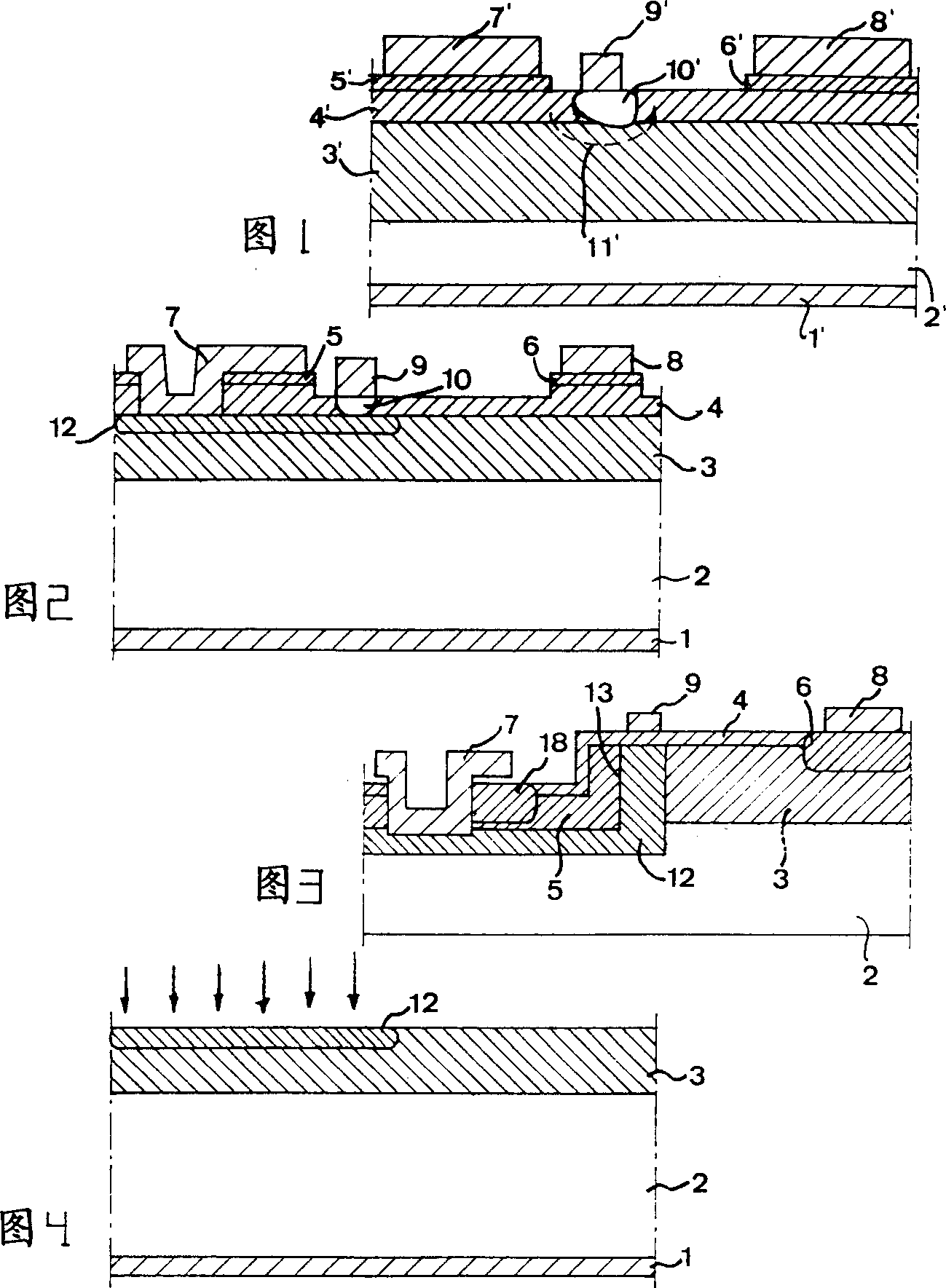
[0031] A brief description of transistors according to the prior art

[0032] The transistor shown in Figure 1 is prior art and has the following silicon carbide layers on top of the backside metallization layer 1': semi-insulating substrate layer 2', p-type buffer layer 3', and n-type channel layer 4' . The buffer layer is employed to minimize the influence of the deep centers present in the semi-insulating substrate on the carrier transport. The doping level of the buffer layer should be low to keep high frequency losses low. The transistor also comprises laterally separated source region layer 5' and drain region layer 6' arranged on top of channel layer 4', heavily doped n-type. Source contacts 7' and drain contacts 8' are arranged on these layers. This transistor also comprises a gate electrode 9' arranged on top of the channel layer 4' between the source layer 5' and the drain layer 6'. When a voltage is applied between the source and drain contacts, current can flow i...


PUM

PropertyMeasurementUnit
Doping concentrationaaaaaaaaaa

Abstract

A lateral field effected transistor of SiC for high switching frequencies comprises a source region layer (5) and a drain region layer (6) laterally spaced and highly doped n-type, an n-type channel layer (4) extending laterally and interconnecting the source region layer and the drain region layer for conducting a current between these layers in the on-state of the transistor, and a gate electrode (9) arranged to control the channel layer to be conducting or blocking through varying the potential applied to the gate electrode. A highly doped p-type base layer (12) is arranged next to the channel layer at least partially overlapping the gate electrode and being at a lateral distance to the drain region layer. The base layer is shorted to the source region layer.

Description

technical field [0001] The present invention relates to a silicon carbide lateral field effect transistor for high switching frequency, which comprises a laterally separated heavily doped n-type source region layer and a drain region layer, a lower doping concentration laterally extending and separating the source region layer an n-type channel layer interconnected with the drain layer to conduct current between these layers when the transistor is in the on state, and arranged to control the properties of the channel layer to be conductive or off by varying the potential applied to the gate electrode gate electrode. Background technique [0002] "High switching frequency" here means higher than 1MHz. Such transistors can be used in eg power microwave applications eg in mobile phone base stations, radar, and microwave ovens. [0003] In order to increase the on-state channel current, minimize the transit time of carriers in the channel and gate capacitance, this type of hig...

Claims


Application Information

Patent Timeline
IPC IPC(8): H01L29/78H01LH01L21/335H01L21/338H01L29/24H01L29/772H01L29/812
CPCH01L21/18
Inventor 克里斯托弗·哈里安德雷·康斯坦丁欧夫
Owner クレースウェーデンアクチボラゲット
Why Eureka
Try Eureka