Periodic metal/dielectric structural photon crystal with three-dimensional band gap and preparing mehtod thereof

A photonic crystal, dielectric structure technology, applied in optics, electrical components, optical components, etc., to achieve the effect of reducing quality and difficulty

Inactive Publication Date: 2004-02-04
NANJING UNIV
View PDF2 Cites 11 Cited by
  • Summary
  • Abstract
  • Description
  • Claims
  • Application Information

AI Technical Summary

Problems solved by technology

The disadvantage is that the med

Method used


Image

  • Periodic metal/dielectric structural photon crystal with three-dimensional band gap and preparing mehtod thereof
  • Periodic metal/dielectric structural photon crystal with three-dimensional band gap and preparing mehtod thereof
  • Periodic metal/dielectric structural photon crystal with three-dimensional band gap and preparing mehtod thereof

Examples


Embodiment Construction

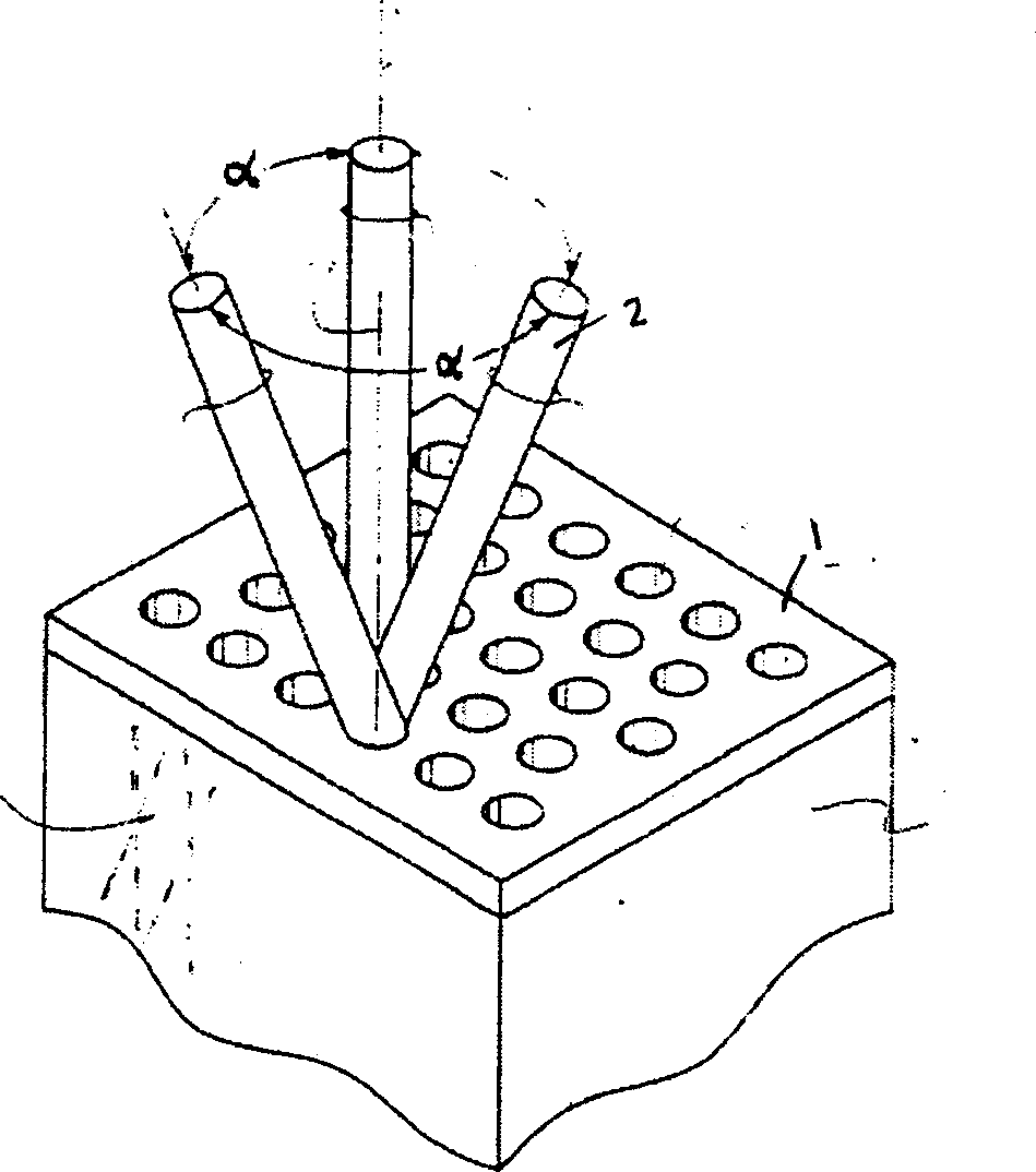
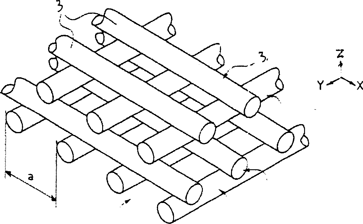
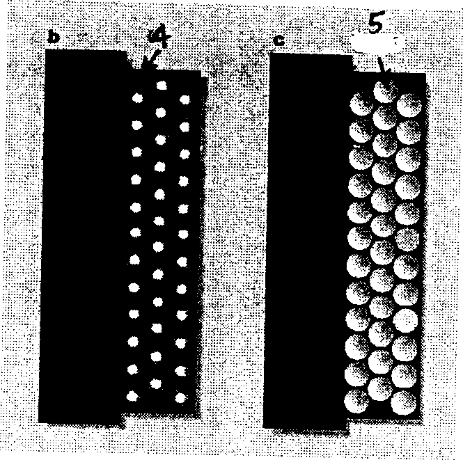
[0039] The most basic unit of the three-dimensional full-bandgap photonic crystal of the present invention is a compound dielectric sphere composed of metal and dielectric material. The schematic diagram of its internal structure is shown in Figure 3A and 4A .

[0040] In the present invention, by implementing a dielectric coating on the surface of a solid metal sphere, a Figure 3A Composite media spheres are shown.

[0041] In the present invention, monodisperse colloidal spheres (such as polystyrene or silicon dioxide) are adopted as the support core, and at first the surface is passed through existing chemical methods: these methods mainly include: surface seed growth technology, referring to S.J.Oldenburg, R.D.Averitt, S.L.Westcott, N.J.Halas, Chem.Phys.Lett.1998, 288, 243; Surface Deposition Reaction Technology, see L.M.Liz-Marzán, M.Giersig, P.Mulvaney, Langmuir 1996, 12, 4329; Surface Chemistry Methods Treatment and Function For mass adsorption methods, see S.L. W...


PUM


Abstract

In the present invention, the composite dielectric ball in metal/dielectric material is arranged according to close-packed mode at three-dimensional space. The core of this composite dielectric ball is spherical metal granule as outer layer is dielectric wrapping layer, or the core is supporting ball made of organic or inorganic material, middle sandwich layer is metal ball shell and outer layer is dielectric wrapping layer.

Description

1. Technical field [0001] The invention relates to a three-dimensional periodic metal / dielectric structure photonic crystal material with a full band gap, in particular a full band gap photonic crystal with a close-packed structure composed of metal / dielectric material composite dielectric spheres and a related preparation method. 2. Background of the invention [0002] Recent discoveries have drawn particular attention to a phenomenon known as the "photonic bandgap," so named because it arises in close resemblance to the so-called electronic "energy gap" in semiconductors. In the following part we call the structural materials with such properties photonic crystals. [0003] Although the application of 1D photonic crystals has been around for a long time, the idea of ​​designing and fabricating 2D and 3D photonic crystals was only developed more than ten years ago. There is growing interest in this type of structure due to its many potential applications. Photonic crystal...

Claims


Application Information

Patent Timeline
IPC IPC(8): G02B1/02G02B5/12G02B5/124H01Q15/14
Inventor 王振林章维益闵乃本
Owner NANJING UNIV
Why Eureka
Try Eureka