

Contact switch and appts. provided with contact switch
A contact switch, contact technology, which is applied to contacts, electrical switches, microstructure devices composed of deformable elements, etc. Deformation reduction and other problems, to ensure contact reliability between contacts, reduce gap deviation, and reduce loss
- Summary
- Abstract
- Description
- Claims
- Application Information
AI Technical Summary
Problems solved by technology
Method used
Image

Examples
Embodiment Construction
[0060] Embodiments of the present invention will be described below with reference to the drawings. In addition, in all drawings of the following embodiment, the same code|symbol is used for the same or corresponding part.
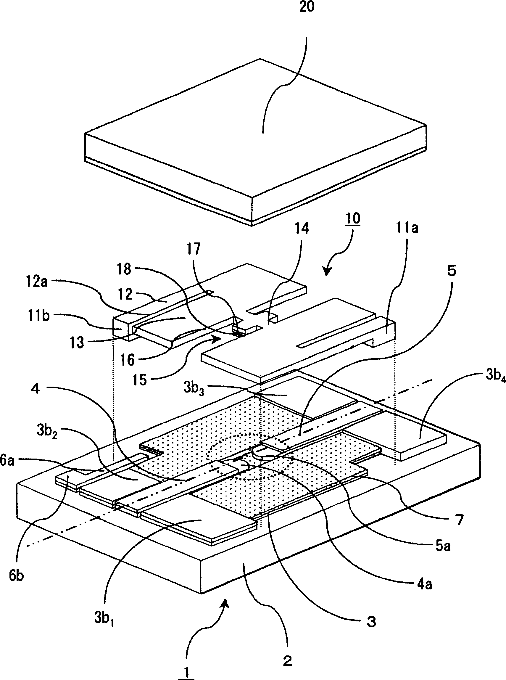
[0061] First, a contact switch according to a first embodiment of the present invention will be described. exist figure 1 In , a micro relay as the contact switch of the first embodiment is shown.
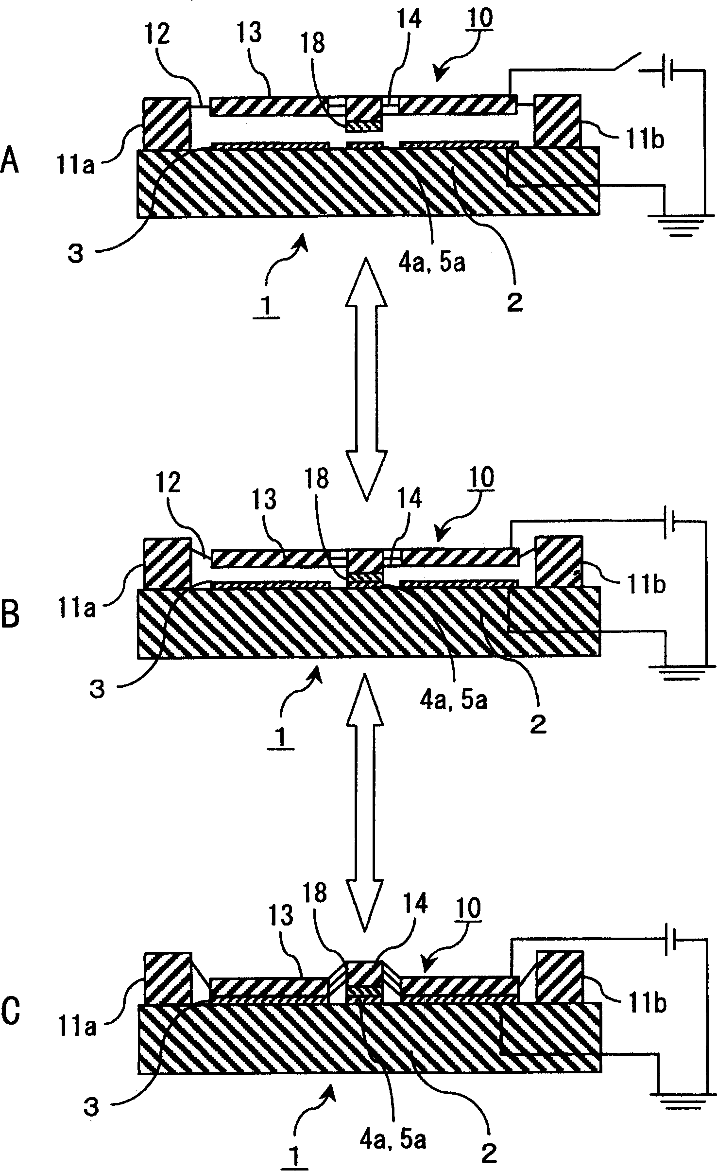
[0062] Such as figure 1 As shown, the electrostatic microrelay of the first embodiment has a structure in which the movable substrate 10 is integrated with a predetermined interval on one surface of the fixed substrate 1, and furthermore, the cover 20 is provided to cover the movable substrate 10. .
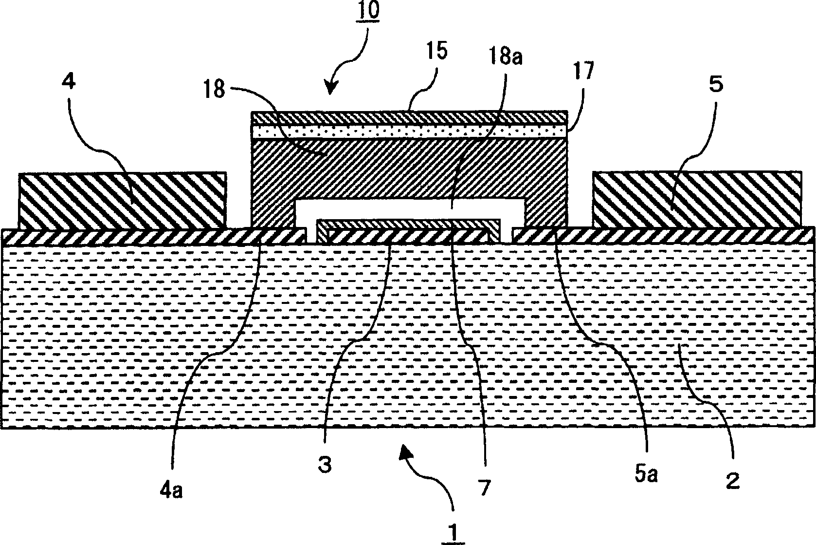
[0063] The fixed substrate 1 is structured such that at least a fixed electrode 3 and two signal lines 4 and 5 are provided on the upper surface of a glass substrate 2 .
[0064] The signal lines 4 and 5 are arranged in the same straight line ( figure 1 o...
PUM
 Abstract
Description
Claims
Application Information