

Using rows/columns of micro-vias in a BGA interconnect grid to create improved PCB routing channels
一种微通孔、连接到的技术,应用在电气连接印刷元件、半导体/固态器件零部件、印刷电路等方向,能够解决器件功能性起负面影响、不合乎要求等问题
- Summary
- Abstract
- Description
- Claims
- Application Information
AI Technical Summary
Problems solved by technology
Method used
Image

Examples
Embodiment Construction
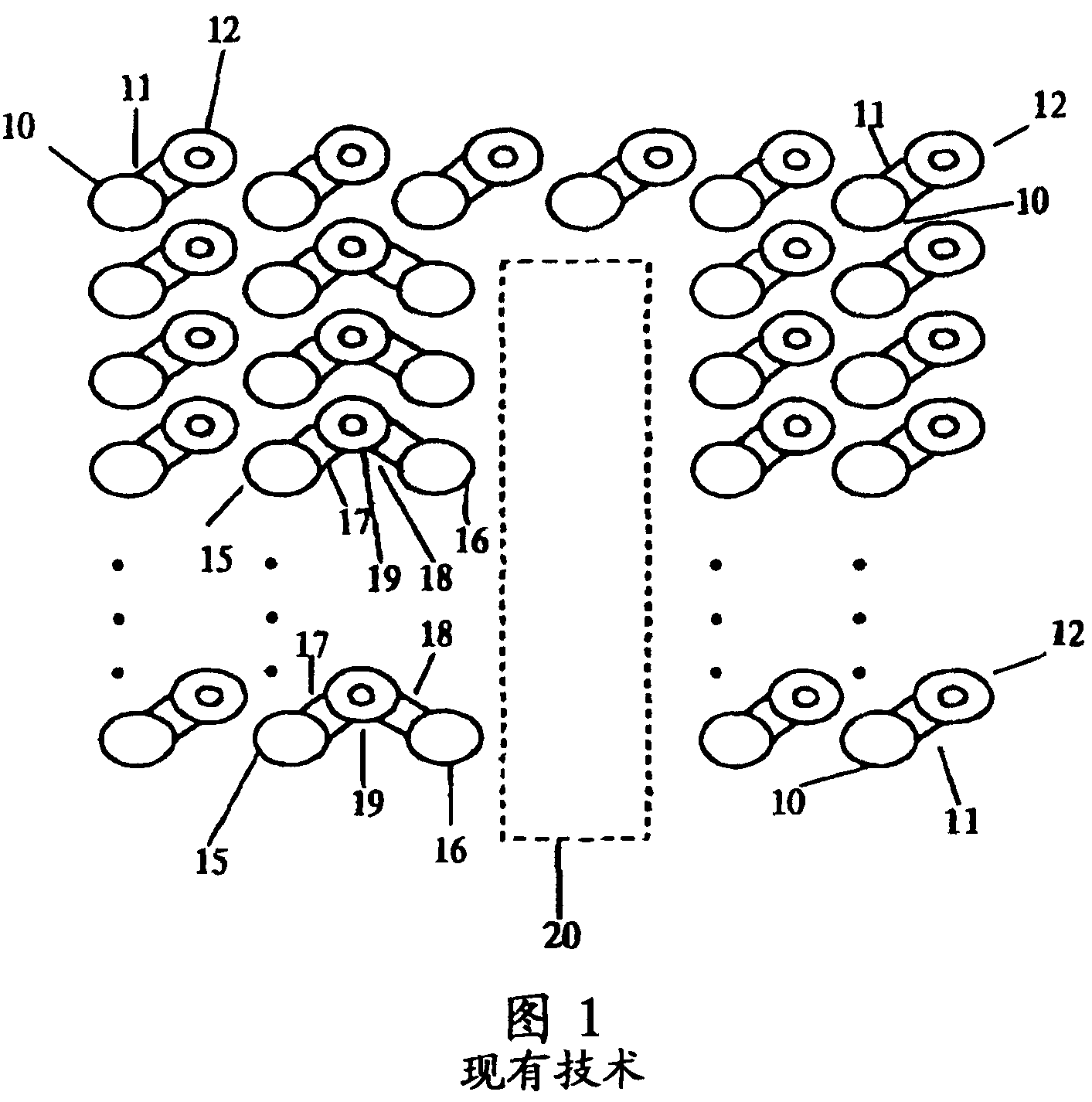
[0022] Figure 1 is a top view of a printed circuit board (PCB) surface incorporating a prior art solution. Ball grid array (BGA) ball contact pads 10 are connected to through-board vias 12 through links 11 . To provide routing channels 20, selected rows of ball contact pads 15 and 16 are connected by links 17 and 18 to a common through-board via 19, which is designated here as a shared through-board via. The disadvantages of this solution are described above.
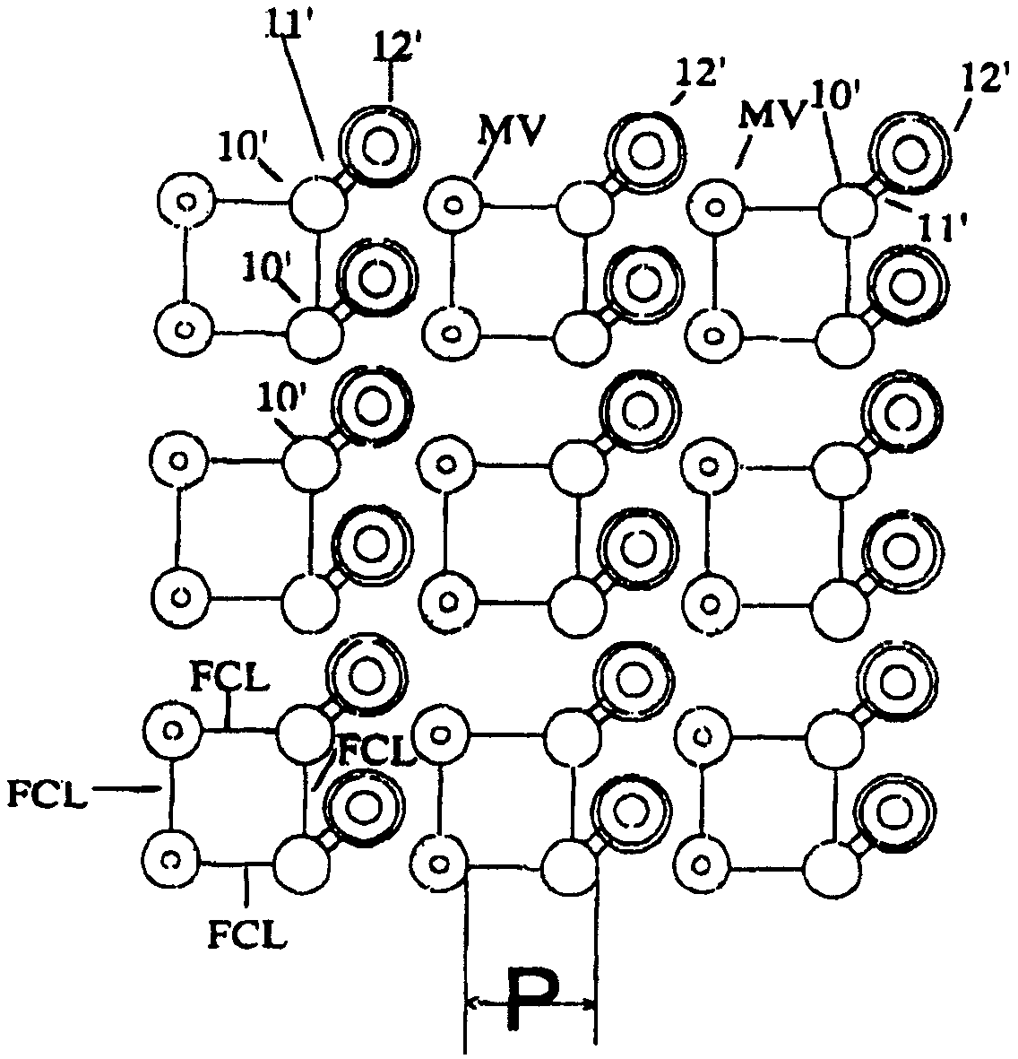
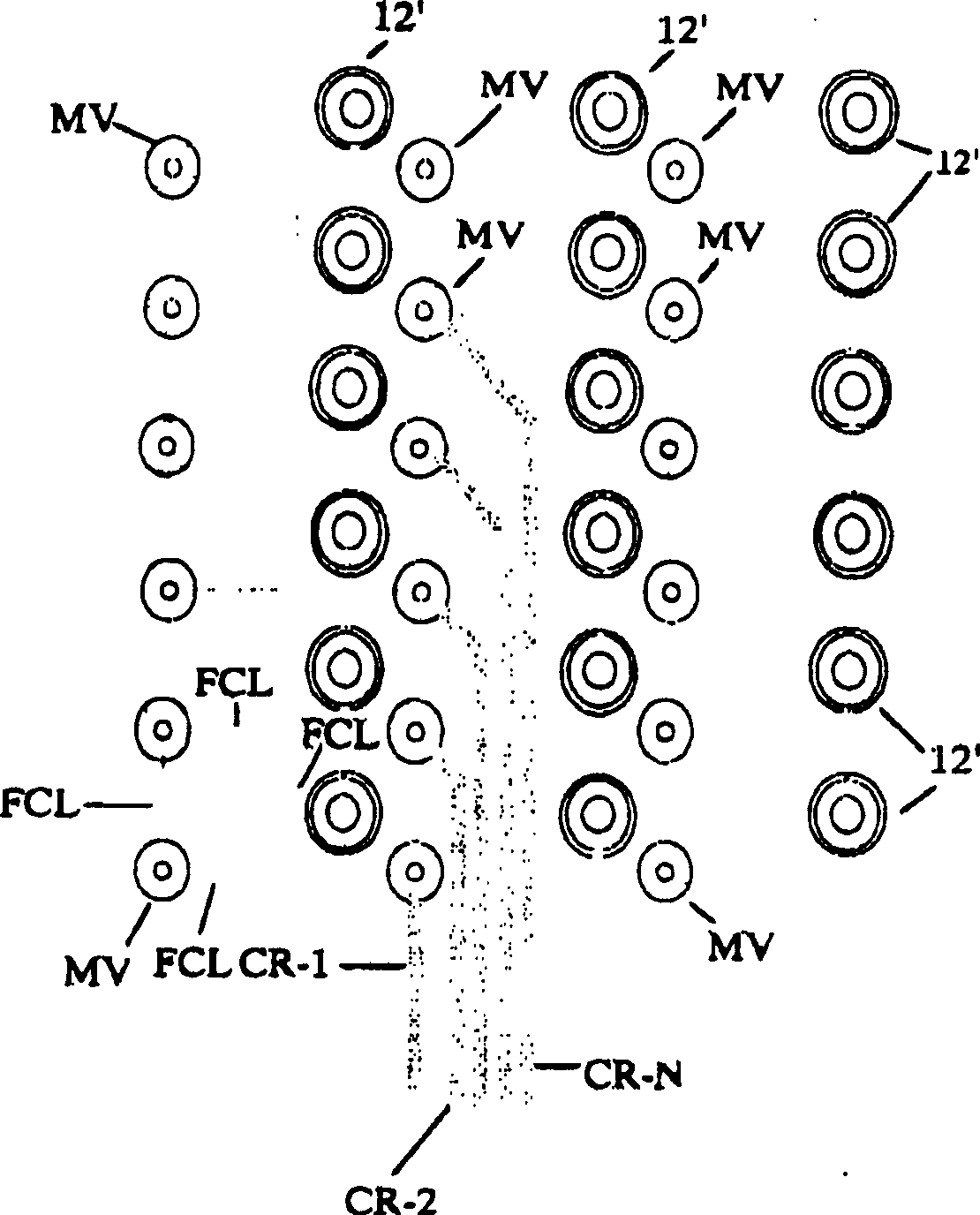
[0023] The invention is Figure 2a , 2b and 2c to illustrate. (Original labeled components correspond to those in Figure 1.) The first three-layer circuit board is shown to illustrate the BGA package specification.
[0024] By creating columns and / or rows of microvias interspersed in columns / rows of regular vias every other row, the columns and rows of vias at these locations can be eliminated. exist Figure 2a , the columns MVC1, MVC2, MVC3... of micro vias are scattered in each column of regular vias C1, C2, C3......
PUM
 Abstract
Description
Claims
Application Information