Chip encapsulation structure and its making method
A technology of chip packaging structure and manufacturing method, which is applied in semiconductor/solid-state device manufacturing, electrical components, electrical solid-state devices, etc.
- Summary
- Abstract
- Description
- Claims
- Application Information
AI Technical Summary
Problems solved by technology
Method used
Image


Examples
Embodiment Construction
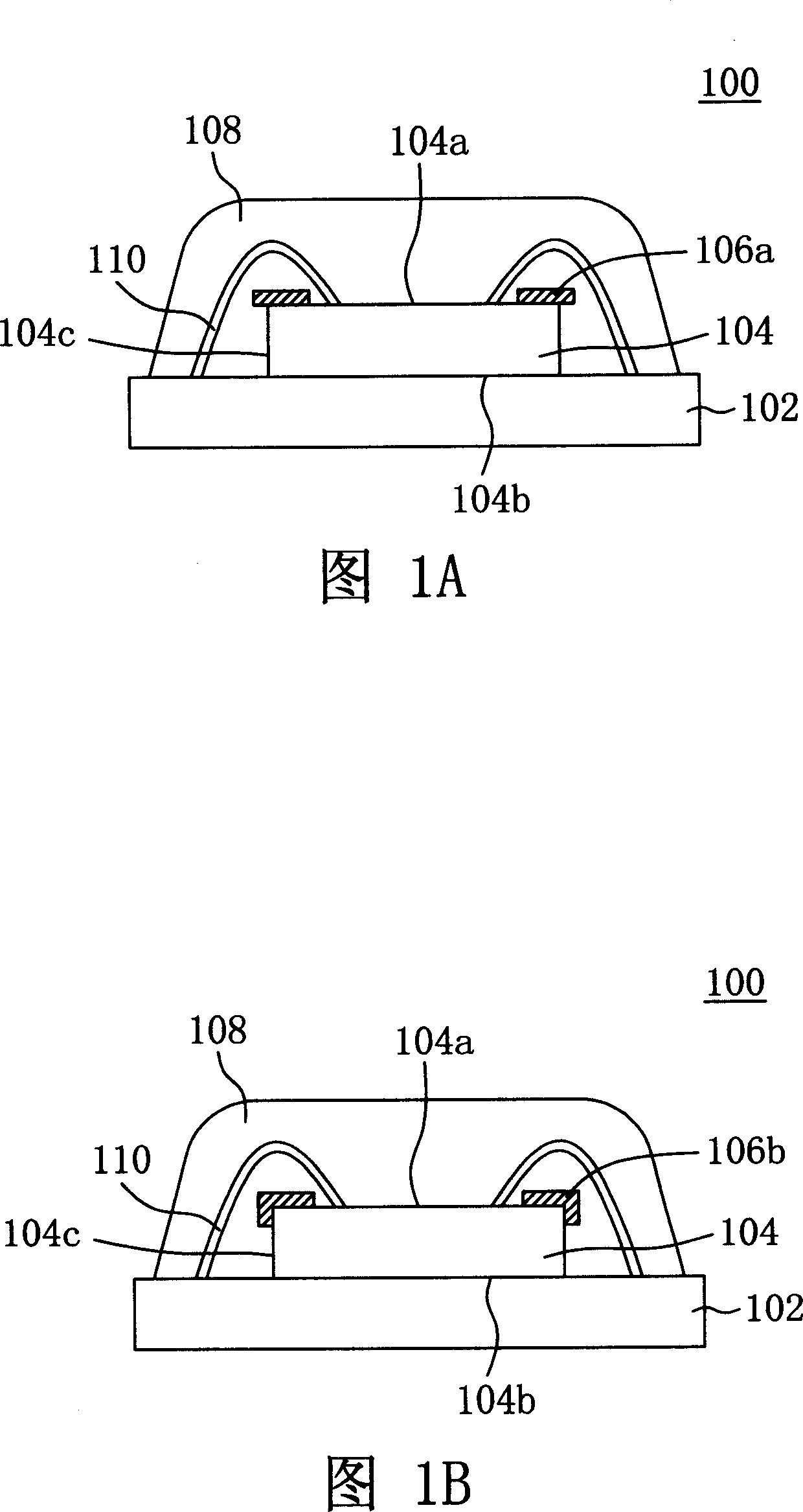
[0011] Please refer to FIGS. 1A and 1B at the same time. FIG. 1A is a schematic cross-sectional view of a chip package structure with a planar annular reinforcement in accordance with the characteristics of the present invention, and FIG. 1B is a chip package with a turning ring reinforcement in accordance with the characteristics of the present invention Schematic cross-sectional view of the structure. As shown in the figure, the chip packaging structure 100 includes a carrier 102, a chip 104, a reinforcement and a glue 108. The carrier 102 is, for example, a substrate, and the chip 104 is, for example, a low-k (low-K) chip. The chip 104 has an upper surface 104a, a lower surface 104b, and an outer sidewall 104c. The lower surface 104b is disposed on the carrier 102. The surface 104a is electrically connected to the carrier 102 through the circuit 110. The reinforcement covers the edge of the upper surface 104a to protect the edge. The way the reinforcement covers this edge is sh...
PUM
 Abstract
Description
Claims
Application Information