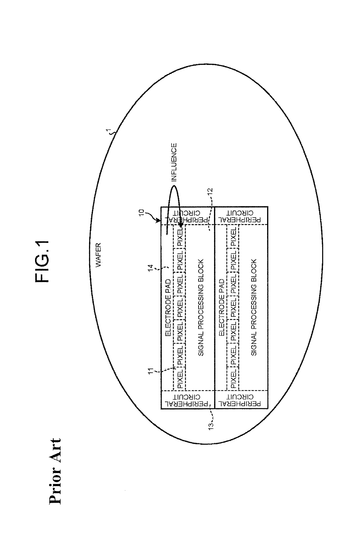
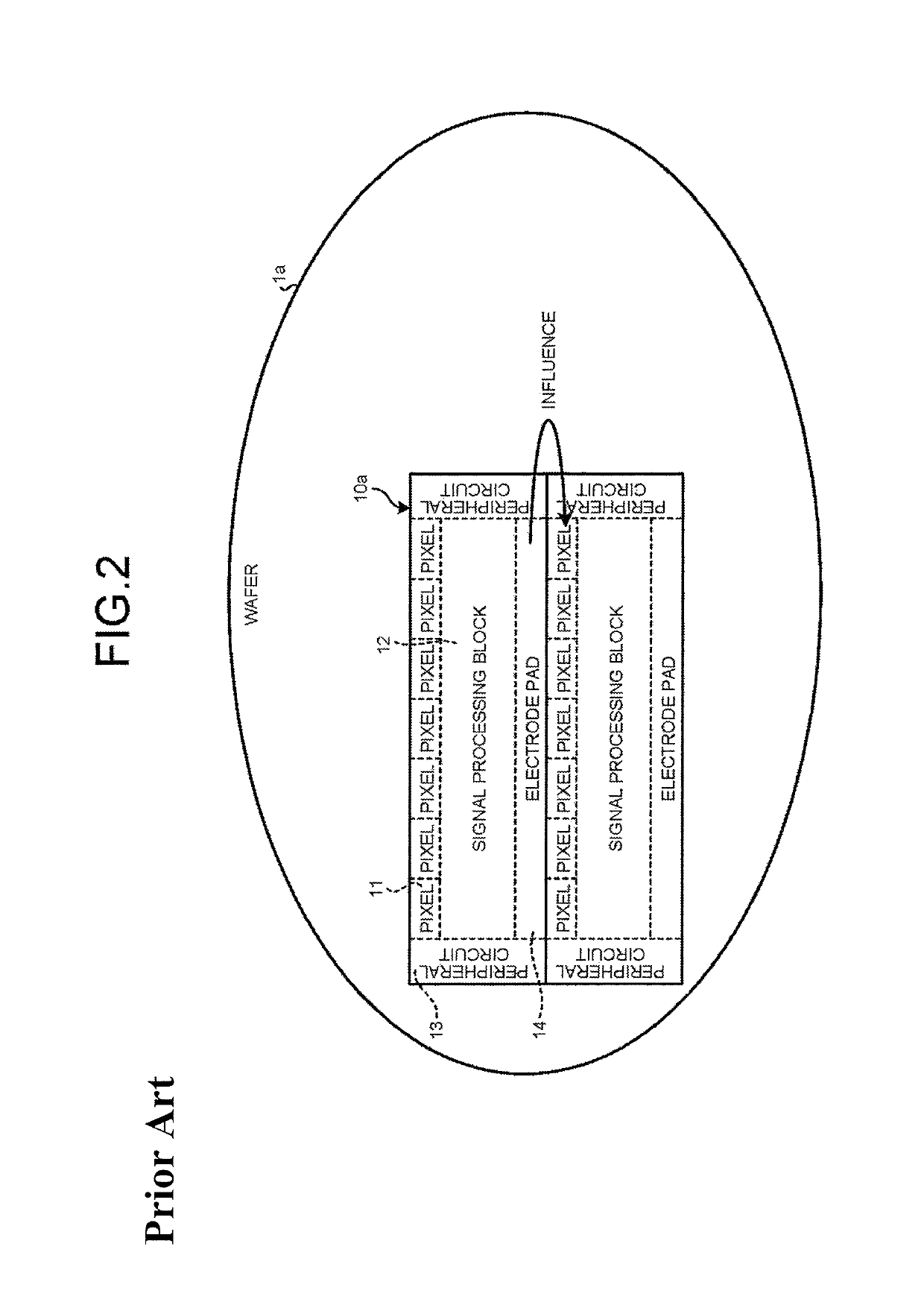
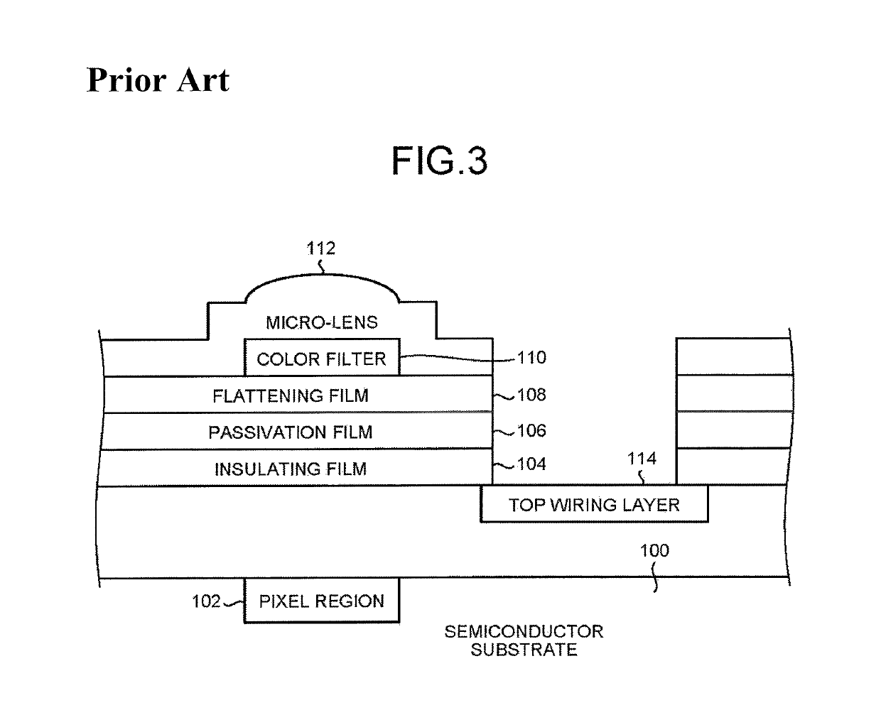
Solid-state imaging device
a solid-state imaging and imaging device technology, applied in the field of imaging devices, can solve the problems of unevenness in the application of color filter pigments and/or in the formation of micro-lenses, image characteristics may be degraded, and resolution varies
- Summary
- Abstract
- Description
- Claims
- Application Information
AI Technical Summary
Problems solved by technology
Method used
Image

Examples
first embodiment
[0031
[0032]Next, a configuration of a solid-state imaging device according to a first embodiment will be explained, with reference to FIGS. 4 and 5. FIG. 4 is a diagram illustrating an exemplary configuration of a solid-state imaging device 2 according to the first embodiment.
[0033]The solid-state imaging device 2 may be, for example, a CMOS color linear sensor and may be installed in an image reading device or a Multifunction Peripheral (MFP) including an image reading device. The solid-state imaging device 2 includes a red (R) light reading unit 20RE, another red (R) light reading unit 20RO, a green (G) light reading unit 20GE, another green (G) light reading unit 20GO, a blue (B) light reading unit 20BE, and another blue (B) light reading unit 20BO. The R light reading unit 20RE includes a pixel 30 as described below with reference to FIG. 5 and is provided with a color filter that transmits red-colored light and an on-chip micro-lens. The R light reading unit 20RO has the same c...
second embodiment
[0064
[0065]Next, a configuration of a solid-state imaging device according to a second embodiment will be explained, with reference to FIG. 11. FIG. 11 is a diagram illustrating an exemplary configuration of a solid-state imaging device 2a according to the second embodiment. The solid-state imaging device 2a is obtained by removing the first current source 22 from the solid-state imaging device 2 illustrated in FIG. 4. Because the solid-state imaging device 2a is not provided with the first current source 22, the direct current caused to flow by the first current source 22 is reduced. In other words, the solid-state imaging device 2a is configured to perform a subthreshold writing process.
[0066]According to at least one aspect of the present invention, an advantageous effect is achieved where it is possible to provide a solid-state imaging device capable of preventing the image reading characteristics from being degraded.
[0067]The above-described embodiments are illustrative and do ...
PUM
 Abstract
Description
Claims
Application Information
 - R&D
- Intellectual Property
- Life Sciences
- Materials
- Tech Scout
- Unparalleled Data Quality
- Higher Quality Content
- 60% Fewer Hallucinations
Browse by: Latest US Patents, China's latest patents, Technical Efficacy Thesaurus, Application Domain, Technology Topic, Popular Technical Reports.
© 2025 PatSnap. All rights reserved.Legal|Privacy policy|Modern Slavery Act Transparency Statement|Sitemap|About US| Contact US: help@patsnap.com