Paste composition and method for forming silicon germanium layer
a technology of silicon germanium and composition, which is applied in the direction of non-conductive materials with dispersed conductive materials, coatings, and inks, can solve the problems of requiring requiring the use of hazardous gas, and the process of epitaxial growth and the process of forming a film by sputtering require a long period of time, so as to achieve safe and easy formation and safe and easy formation
- Summary
- Abstract
- Description
- Claims
- Application Information
AI Technical Summary
Benefits of technology
Problems solved by technology
Method used
Image
Examples
example 1
[0085]The following starting materials were prepared.
[0086]Aluminum powder: produced by Toyo Aluminium K.K.; a spherical powder with an aluminum content of 99.9 mass % and an average particle size of 4 μm
[0087]Germanium powder: Ge Powder (produced by Furuuchi Chemical Corporation; a non-spherical powder with a germanium content of 99.999 mass % and an average particle size of 10 μm)
[0088]Resin component: ethyl cellulose resin (produced by Dow)
[0089]A paste composition was prepared using the above starting materials. Specifically, the composition was prepared by adding 47 parts by weight of the germanium powder, 1 part by mass of the ethyl cellulose resin as the resin component, and 15 parts by mass of a diethylene glycol monobutyl ether as a dispersion medium to 100 parts by mass of the aluminum powder.
[0090]The paste composition prepared was applied in an amount of 7 mg / cm2 to a p-type silicon substrate to a thickness of 180 μm.
[0091]Subsequently, after the dispersion medium was re...
example 2
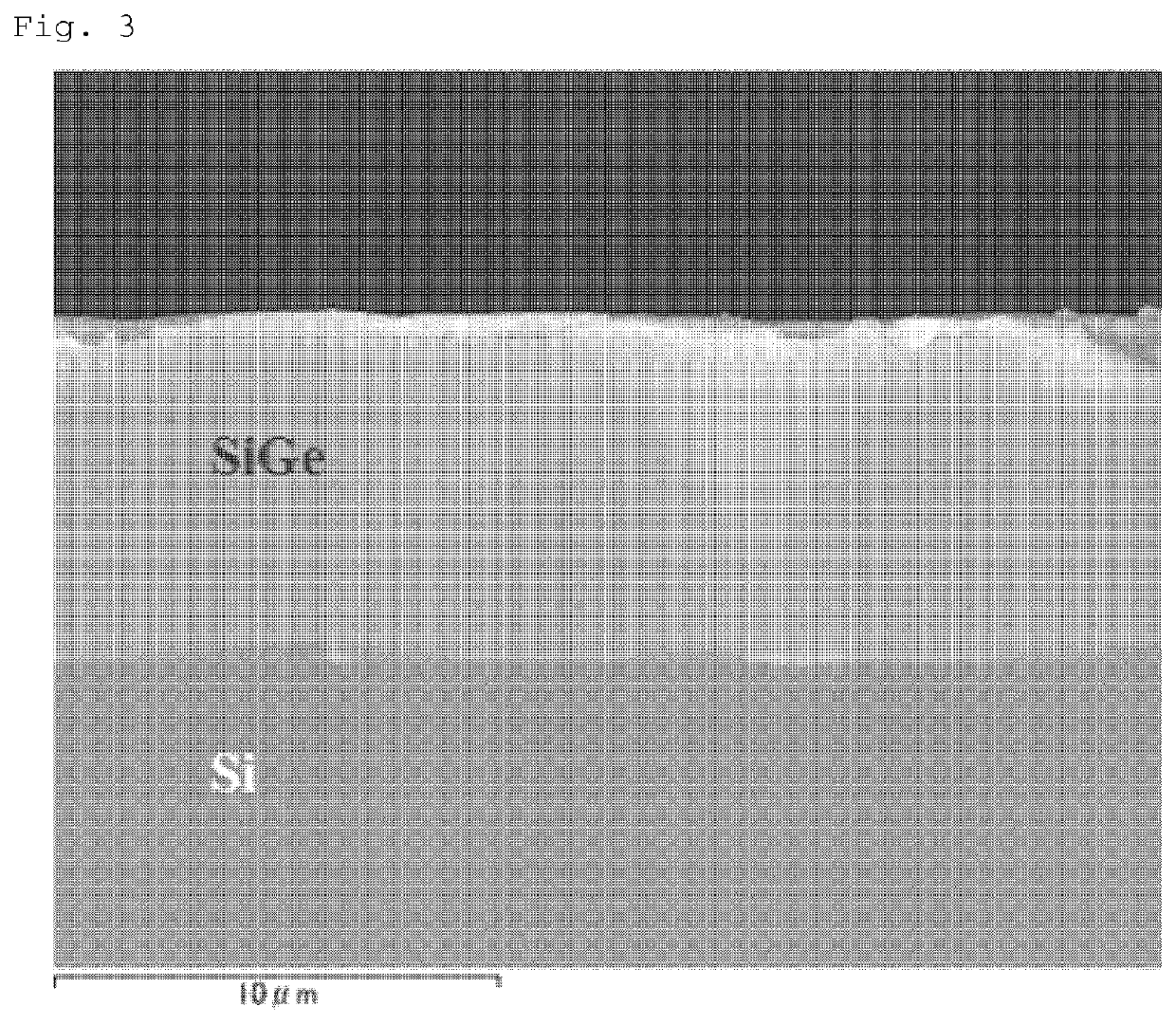
[0094]A laminate in which a silicon germanium layer (Si—Ge layer) was formed on a p-type silicon substrate was produced in the same manner as in Example 1, except that the preheating time was 300 seconds and that sintering was performed for a heating time of 300 seconds.
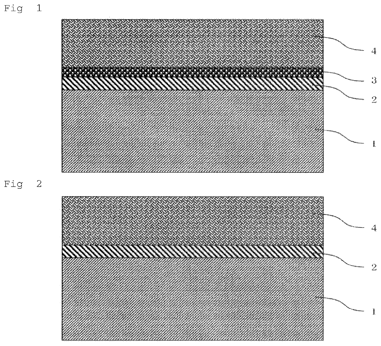
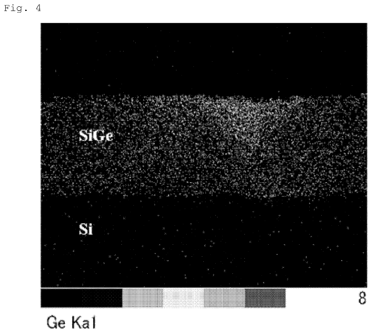
[0095]As in Example 1, it was confirmed that a silicon germanium layer (Si—Ge layer), an aluminum-silicon germanium layer (Al—Si—Ge layer), and an aluminum germanium sintered body layer (Al—Ge sintered body layer) were formed in this order from below on a p-type silicon substrate by sintering. The thickness of the silicon germanium layer varied depending on the measurement point, and the maximum thickness was 16.0 μm.
example 3
[0096]A paste composition was prepared in the same manner as in Example 1, except that the amount of the germanium powder was 9 parts by mass, per 100 parts by mass of the aluminum powder, and a laminate in which a silicon germanium layer (Si—Ge layer) was formed on a p-type silicon substrate was produced.
[0097]As in Example 1, it was confirmed that a silicon germanium layer (Si—Ge layer), an aluminum-silicon germanium layer (Al—Si—Ge layer), and an aluminum germanium sintered body layer (Al—Ge sintered body layer) were formed in this order from below on a p-type silicon substrate by sintering. The thickness of the silicon germanium layer varied depending on the measurement point, and the maximum thickness was 4.9 μm.
PUM
| Property | Measurement | Unit |
|---|---|---|
| temperature | aaaaa | aaaaa |
| particle size | aaaaa | aaaaa |
| particle size | aaaaa | aaaaa |
Abstract
Description
Claims
Application Information


