Device and method for measuring thickness of dielectric layer in circuit board

a dielectric layer and circuit board technology, applied in the direction of measurement devices, instruments, structural/machine measurement, etc., can solve the problems of circuit board scrapping, high cost, and high labor intensity of prior ar

Active Publication Date: 2022-08-09
UNIMICRON TECH CORP
View PDF14 Cites 0 Cited by
  • Summary
  • Abstract
  • Description
  • Claims
  • Application Information

AI Technical Summary

Benefits of technology

[0004]The objective of the present invention is to provide a method for measuring a thickness of a dielectric layer in a circuit board. The method for measuring the thickness of the dielectric layer in the circuit board can quickly and easily measure the thickness of the dielectric layer in the circuit board without damaging the circuit board.
[0012]Another objective of the present invention is to provide a measuring device. The measuring device can quickly and easily measure a thickness of a dielectric layer in a circuit board without damaging the circuit board.
[0020]Only by forming a through hole in the pre-set test area, the measuring device can be moved into the through hole to shoot the dielectric layer of the circuit board. The required area of the circuit board is small, and the circuit board will not be damaged.

Problems solved by technology

Currently, the thickness of the dielectric layer of the circuit board is mainly measured by destructive methods.
However, such prior art is very time-consuming and labor-intensive, and it will also damage a larger area of the circuit board and cause the circuit board to be scrapped.

Method used


Image

  • Device and method for measuring thickness of dielectric layer in circuit board
  • Device and method for measuring thickness of dielectric layer in circuit board
  • Device and method for measuring thickness of dielectric layer in circuit board

Examples


Embodiment Construction

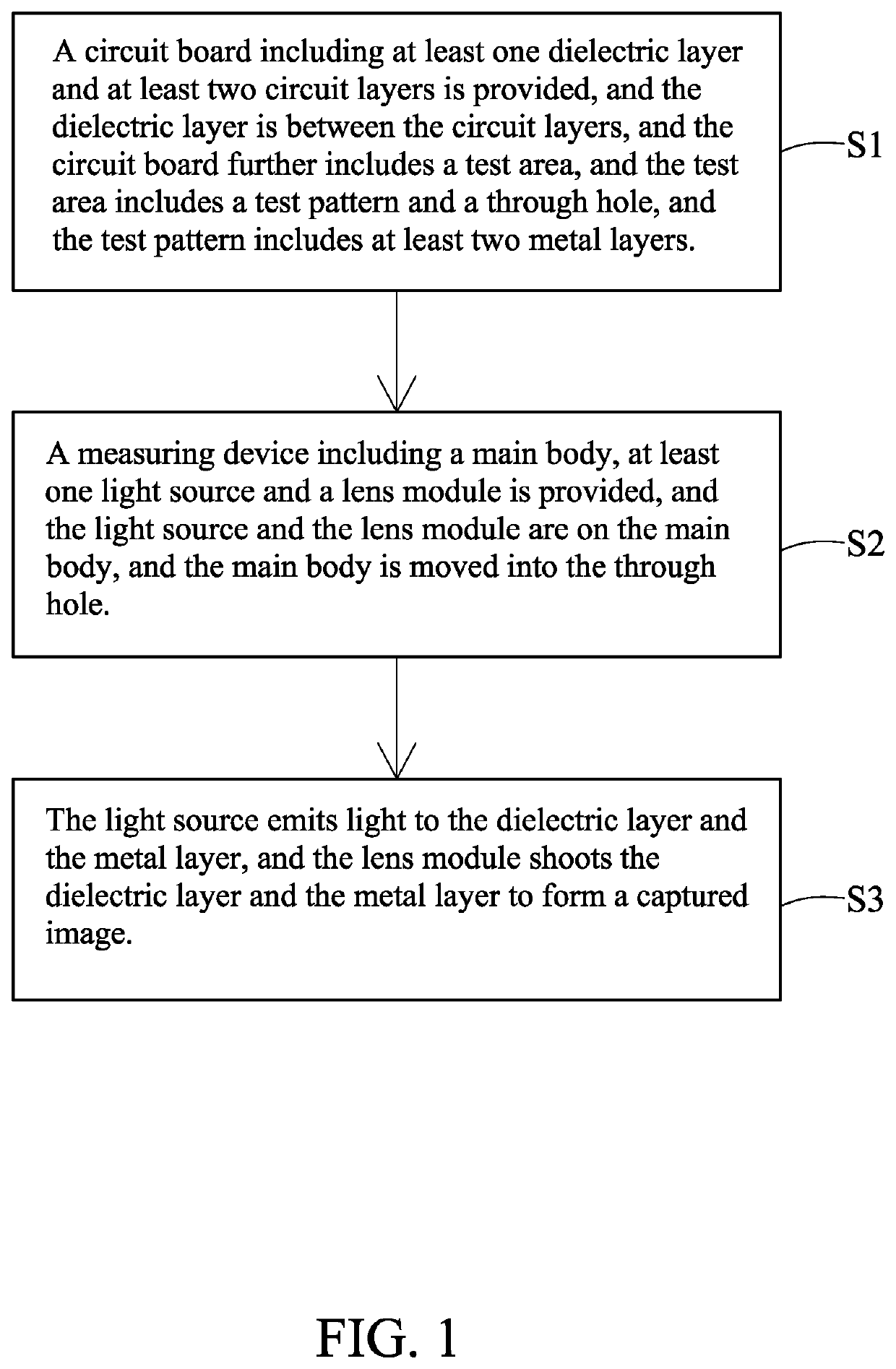
[0029]Please refer to FIG. 1. FIG. 1 illustrates a schematic diagram of a method for measuring a thickness of a dielectric layer in a circuit board of the present invention. The method for measuring the thickness of the dielectric layer in the circuit board in the present invention includes the following steps.

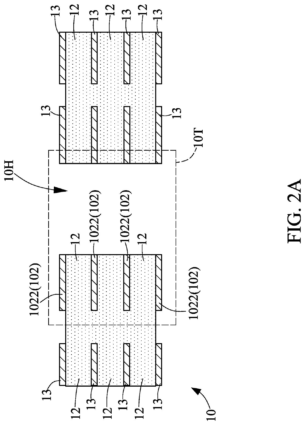
[0030]First, please refer the step S1 and FIG. 2A. FIG. 2A illustrates a schematic diagram of a partial section of a circuit board 10. A circuit board 10 including three dielectric layers 12 and four circuit layers 13 is provided. However, person having ordinary skill in the art should understand that in practice, the circuit board 10 may include more dielectric layers 12 and circuit layers 13, or the circuit board 10 may only include one dielectric layer 12 and two circuit layers 13. Moreover, the dielectric layer 12 is between the two circuit layers 13.

[0031]In addition, the circuit board 10 further includes a test area 10T, and the test area 10T includes a test pattern 102 ...


PUM

PropertyMeasurementUnit
thicknessaaaaaaaaaa
optical microscopeaaaaaaaaaa
scanning electron microscopeaaaaaaaaaa

Abstract

A method for measuring a thickness of a dielectric layer in a circuit board is provided. The method for measuring the thickness of the dielectric layer includes the following steps. First, a circuit board including at least one dielectric layer and at least two circuit layers is provided. The dielectric layer is between the circuit layers, and the circuit board further includes a test area including a test pattern and a through hole. The test pattern includes at least two metal layers. Next, a measuring device including a main body, at least one light source and a lens module is provided. When the main body is moved into the through hole, the light source emits light to the dielectric layer and the metal layer, and the lens module shoots the dielectric layer and the metal layer to form a captured image. The thickness of the dielectric layer is obtained via the captured image.

Description

FIELD OF THE DISCLOSURE[0001]The present invention relates to a device and a method for measuring a thickness of a dielectric layer in a circuit board, and more particularly to the device and the method for measuring the thickness of the dielectric layer in the circuit board including a light source and a lens module.BACKGROUND OF THE INVENTION[0002]Currently, the thickness of the dielectric layer of the circuit board is mainly measured by destructive methods. For example, partial circuit board must be removed to be a measuring slice, firstly. Next, using optical microscope or scanning electron microscope to measure the thickness. However, such prior art is very time-consuming and labor-intensive, and it will also damage a larger area of the circuit board and cause the circuit board to be scrapped.[0003]Therefore, how to measure the thickness of the dielectric layer in the circuit board quickly and easily is worth considering for person having ordinary skill in the art.SUMMARY OF TH...

Claims


Application Information

Patent Timeline
Patent Type & Authority Patents(United States)
IPC IPC(8): G01M11/02G01B11/06
CPCG01M11/0207G01B11/06
Inventor CHANG, CHENG-JUICHANG, HUNG-LIN
Owner UNIMICRON TECH CORP
Why Eureka
Try Eureka