Optoelectronic component and optoelectronic arrangement with an optoelectronic component

a technology of optoelectronic components and optoelectronic arrangements, which is applied in the direction of optical elements, instruments, and semiconductor/solid-state device details, can solve the problems of attenuation and interference of detected signals, and achieve good signal properties

Inactive Publication Date: 2005-03-17
INFINEON TECH AG
View PDF3 Cites 26 Cited by
  • Summary
  • Abstract
  • Description
  • Claims
  • Application Information

AI Technical Summary

Benefits of technology

[0004] The present invention is directed to an optoelectronic component which is distinguished by good signal properties and a compact construction. Furthe

Problems solved by technology

Relatively long signal paths between the photodiodes and the respectively associated amplifier devices are disadvantageously r

Method used


Image

  • Optoelectronic component and optoelectronic arrangement with an optoelectronic component
  • Optoelectronic component and optoelectronic arrangement with an optoelectronic component
  • Optoelectronic component and optoelectronic arrangement with an optoelectronic component

Examples


Embodiment Construction

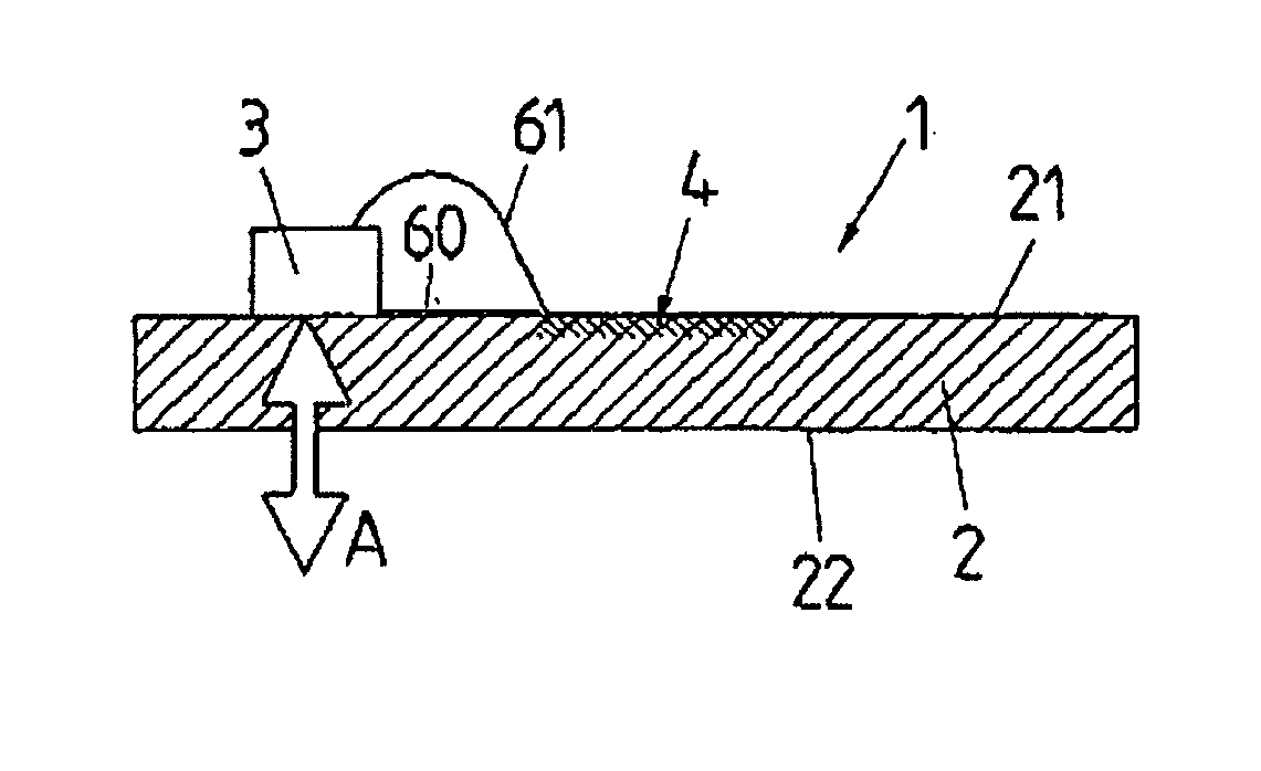
[0041]FIG. 1 schematically shows an optoelectronic component 1 with an optically transparent carrier substrate 2 (also referred to as a submount), an optoelectronic transducer device 3 arranged on the carrier substrate and a circuit 4 which is integrated in the carrier substrate and is electrically connected to the optoelectronic transducer device 3.

[0042] The optically transparent carrier substrate 2 is transparent at least for wavelengths which the transducer device 3 receives or transmits. Coupling of light signals takes place from the back side 22 of the carrier substrate through the carrier substrate to or from the front side 21, on which the transducer device 3 is located, cf. arrow A. Silicon is used for example as the carrier substrate for infrared light or sapphire is used as the carrier substrate for visible light. The materials referred to for the carrier substrate 4 additionally have the advantage that they provide good heat removal, which is advantageous in particular ...


PUM


Abstract

An optoelectronic component with an optoelectronic transducer device and an electrical circuit electrically connected to the transducer device mounted on a carrier substrate which is optically transparent for specific wavelengths. The transducer device is arranged on the front side of the carrier substrate, and light coupling takes place through the back side. The electrical circuit is formed as a circuit integrated into the carrier substrate or is formed on the carrier substrate using hybrid technology, the terminal contacts of the circuit being arranged on the front side of the carrier substrate. An optoelectronic arrangement with an optoelectronic component includes an at least partly planar-formed mounting element, which is connected by its one side to an outer side of the component or is integrated in the latter and extends at least as far as an outer edge of the component, and includes a mechanical interface for the mechanical connection of the component.

Description

FIELD OF THE INVENTION [0001] The invention relates to an optoelectronic component, and in particular to the construction of a surface-mountable optoelectronic component and its connection to further components. BACKGROUND OF THE INVENTION [0002] DE 102 01 102 A1 discloses an optoelectronic component in which a laser diode is arranged on an optically transparent carrier substrate, through which the light signal generated is emitted. The contacting of the laser diode and further components takes place by means of a leadframe. The arrangement is surrounded by a plastic package. [0003] In the case of DE 41 06 721 A1, a number of photodiodes and associated amplifier devices are arranged on the surface of a carrier substrate. Relatively long signal paths between the photodiodes and the respectively associated amplifier devices are disadvantageously required, leading to an attenuation and interference of the detected signal, in particular at high frequencies in the GHz range. SUMMARY OF T...

Claims


Application Information

Patent Timeline
IPC IPC(8): G02B6/42H01L23/12H01L23/28H01L23/50H01L29/16H01L29/267H01L31/0203H01L31/12H01L33/00
CPCG02B6/4201H01L31/0203H01L2224/48247H01L2924/30107H01L2924/00H01L2924/181H01L2224/48091H01L2924/00012H01L2924/00014
Inventor ALTHAUS, HANS-LUDWIGKILLER, THOMASWEIGERT, MARTIN
Owner INFINEON TECH AG
Why Eureka
Try Eureka