Optical transmitter

a technology of optical transmitters and transmitters, applied in the field of infrared communication systems, can solve the problems of pdas and cellular phones, battery exhaustion and breakdown of light-emitting diodes, etc., and achieve the effect of preventing battery exhaustion and breakdown of light-emitting devices and low cos

Inactive Publication Date: 2005-03-24
PANASONIC CORP
View PDF0 Cites 5 Cited by
  • Summary
  • Abstract
  • Description
  • Claims
  • Application Information

AI Technical Summary

Benefits of technology

The present invention is intended to provide an optical transmitter capable of automatically stopping the light-emitting operation of a light-emitting device when the pulse width of an optical transmission input signal exceeds a predetermined value owing to a mal...

Problems solved by technology

Hence, it has been pointed out that various problems, such as battery exhaustion and breakdown of the light-emitting diode 54, may occur in PDAs and cellular phones.
As a result, various problems, such as battery exhaustion and breakdown of the light-emi...

Method used


Image

  • Optical transmitter
  • Optical transmitter
  • Optical transmitter

Examples


first embodiment

( Corresponding to Claims 1, 2, 3 and 5)

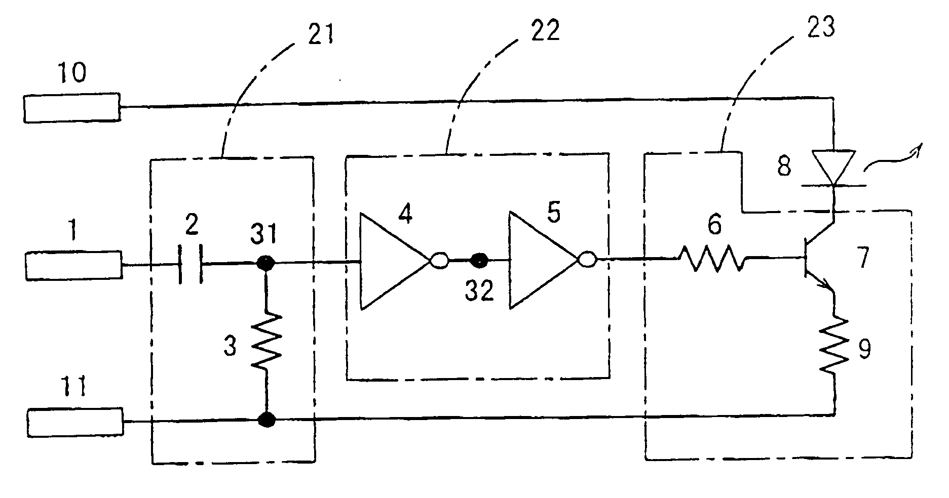
FIG. 1 is a circuit diagram showing the configuration of an optical transmitter in accordance with a first embodiment of the present invention. As shown in FIG. 1, this optical transmitter comprises a high-pass filter 21 for passing the high-frequency components of an optical transmission input signal having a rectangular pulse waveform, a binary circuit 22 for binarizing the output signal of the high-pass filter 21 so as to be returned to a pulse waveform, a light-emitting diode 8 serving as a light-emitting device for optical transmission, and a light-emitting device driving circuit 23 for driving the light-emitting diode 8 depending on the output signal of the binary circuit 22.

The high-pass filter 21 comprises an L-type circuit including a capacitor 2 and a resistor 3, for example.

The binary circuit 22 comprises two-stage inverters 4 and 5 connected in series, for example. The inverters 4 and 5 are each formed of a bipolar transistor, ...

second embodiment

( Corresponding to Claim 7)

FIG. 4 is a circuit diagram showing the configuration of an optical transmitter in accordance with a second embodiment of the present invention. As shown in FIG. 4, in this optical transmitter, the configuration of a light-emitting device driving circuit 24 differs from that of the light-emitting device driving circuit 23 shown in FIG. 1. In other words, in this light-emitting device driving circuit 24, an N-channel MOS transistor 12 is used instead of the NPN bipolar transistor 7. The other configurations are similar to those of the optical transmitter shown in FIG. 1.

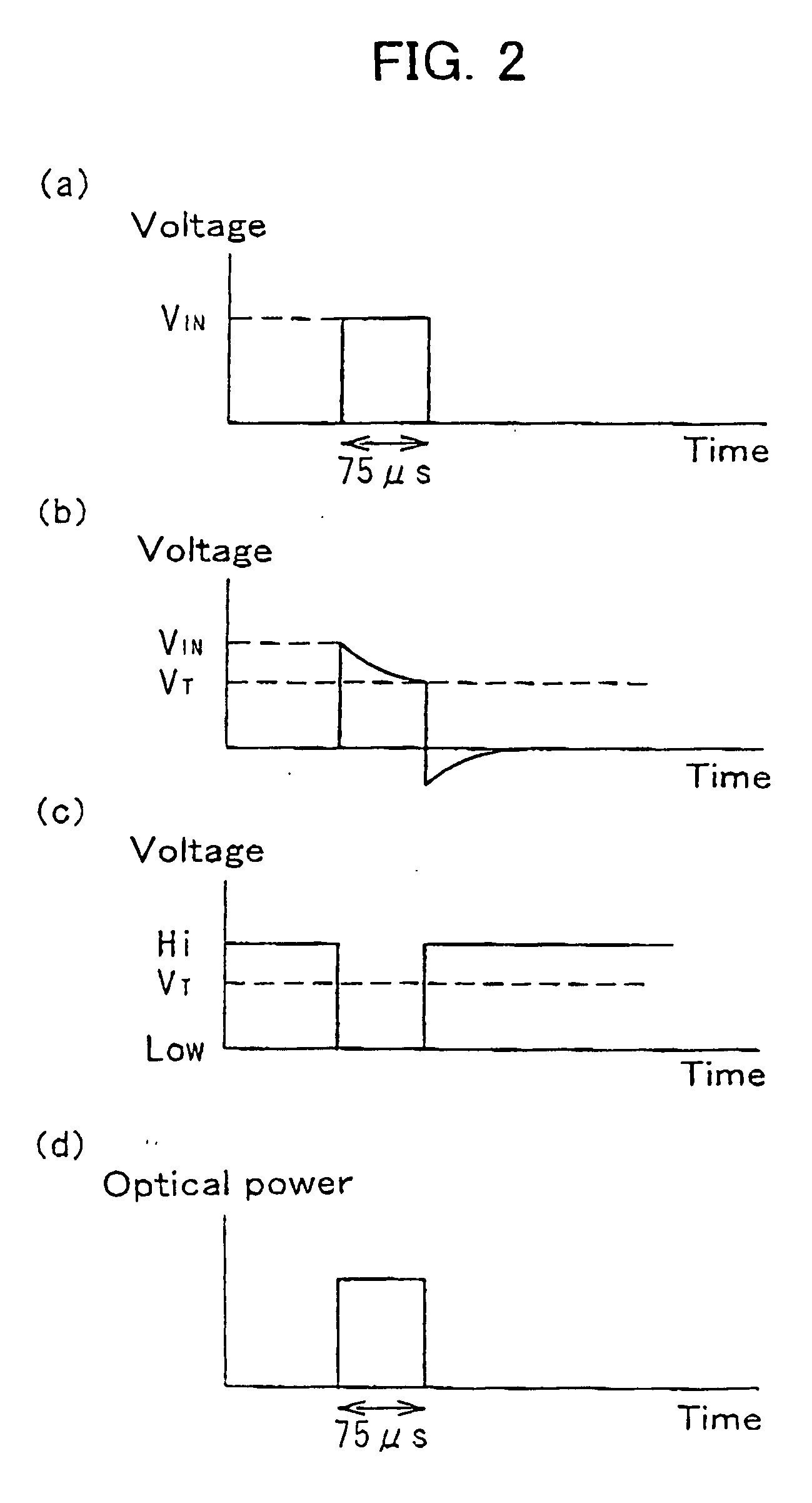
In the circuit diagram of FIG. 1, the operating voltage of the optical transmitter is determined by the forward voltage of the light-emitting diode 8, the terminal voltage of the resistor 9 and the collector-emitter voltage of the NPN bipolar transistor 7.

Since the operating current of the light-emitting diode 8 is determined by light emission power, it is assumed herein that the current...

third embodiment

( Corresponding to Claim 6)

FIG. 5 is a circuit diagram showing the configuration of an optical transmitter in accordance with a third embodiment of the present invention. As shown in FIG. 5, in this optical transmitter, the configuration of a light-emitting device driving circuit 25 differs from that of the light-emitting device driving circuit 23 shown in FIG. 1. In other words, in this light-emitting device driving circuit 25, instead of the one-stage NPN bipolar transistor 7, a Darlington circuit having a two-stage configuration wherein NPN bipolar transistors 17 and 7 are connected in series is used. In this light-emitting device driving circuit 25, depending on the output signal of the binary circuit 22, input to the base of the first-stage NPN bipolar transistor 17, the next-stage NPN bipolar transistor 7 interrupts the current supplied to the light-emitting diode 8.

More specifically, the base of the first-stage NPN bipolar transistor 17 is connected to the other terminal of...


PUM


Abstract

The present invention is intended to prevent a light-emitting diode from emitting light continuously in the case when the level at an input terminal is fixed high because of software or the like and to avoid various problems, such as battery exhaustion and breakdown of the light-emitting diode, in PDAs, cellular phones, etc. For these purposes, a high-pass filter 21 for passing the high-frequency components of an optical transmission input signal having a pulse waveform and a binary circuit 22 for binarizing the output signal of the high-pass filter 21 so as to be returned to a pulse waveform are provided in the preceding stage of a light-emitting device driving circuit 23 for driving a light-emitting diode 8 for optical transmission.

Description

TECHNICAL FIELD Infrared communication systems are widely used for information communication apparatuses, such as notebook personal computers, cellular phones, PDAs (Personal Digital Assistants). Such an infrared communication system comprises a light receiving / emitting module and a system LSI for electrically processing data. The light receiving / emitting module has an optical transmitter for optically transmitting data and an optical receiver for optically receiving data in one package. Although various standards have been proposed for the infrared communication systems, an infrared communication system wherein the IrDA standard is adopted is mainstream in these years. The present invention relates to an optical transmitter for use in the configuration of the above-mentioned infrared communication system. BACKGROUND TECHNOLOGY The above-mentioned conventional optical transmitter has a circuit configuration shown in FIG. 7. In other words, as shown in FIG. 7, an input terminal ...

Claims


Application Information

Patent Timeline
IPC IPC(8): H04B1/04H04B10/40H04B10/50H04B10/524H04B10/60
CPCH04B10/504H04B10/50H04B10/114
Inventor OHSAWA, KATSUICHISHIMAZAKI, TOYOYUKICHATO, TETSUOSHIMIZU, YUZOIMAIZUMI, KENJI
Owner PANASONIC CORP
Why Eureka
Try Eureka